- 您现在的位置:买卖IC网 > PDF目录17066 > DC746A (Linear Technology)BOARD DELTA SIGMA ADC LTC2412 PDF资料下载
参数资料
| 型号: | DC746A |
| 厂商: | Linear Technology |
| 文件页数: | 10/36页 |
| 文件大小: | 0K |
| 描述: | BOARD DELTA SIGMA ADC LTC2412 |
| 软件下载: | QuikEval System |
| 设计资源: | DC746A Design File DC746A Schematic |
| 标准包装: | 1 |
| 系列: | QuikEval™ |
| ADC 的数量: | 1 |
| 位数: | 24 |
| 采样率(每秒): | 7.5 |
| 数据接口: | MICROWIRE?,串行,SPI? |
| 工作温度: | 0°C ~ 70°C |
| 已用 IC / 零件: | LTC2412 |
| 已供物品: | 板 |
| 相关产品: | DC590B-ND - BOARD DEMO USB SERIAL CONTROLLER LTC2412IGN#PBF-ND - IC ADC 2CH DIFF-IN 24BIT 16SSOP LTC2412IGN#TRPBF-ND - IC ADC 2CH DIFF-IN 24BIT 16SSOP LTC2412CGN#TRPBF-ND - IC ADC 2CH DIFF-IN 24BIT 16SSOP LTC2412CGN#PBF-ND - IC ADC 2CH DIFF-IN 24BIT 16SSOP LTC2412IGN#TR-ND - IC CONV A/D 24B 2CH DIFF 16-SSOP LTC2412CGN#TR-ND - IC CONV A/D 24B 2CH DIFF 16-SSOP LTC2412IGN-ND - IC CONV A/D 24B 2CH DIFF 16-SSOP LTC2412CGN-ND - IC ADC 2CH DIFF-IN 24BIT 16SSOP |
第1页第2页第3页第4页第5页第6页第7页第8页第9页当前第10页第11页第12页第13页第14页第15页第16页第17页第18页第19页第20页第21页第22页第23页第24页第25页第26页第27页第28页第29页第30页第31页第32页第33页第34页第35页第36页
LTC2412
18
2412f
APPLICATIO S I FOR ATIO
WU
U
The serial data output pin (SDO) is Hi-Z as long as CS is
HIGH. At any time during the conversion cycle, CS may be
pulled LOW in order to monitor the state of the converter.
While CS is pulled LOW, EOC is output to the SDO pin.
EOC = 1 while a conversion is in progress and EOC = 0 if
the device is in the sleep state. With CS high, the device
automatically enters the low power sleep state once the
conversion is complete.
When the device is in the sleep state (EOC = 0), its
conversion result is held in an internal static shift regis-
ter. Data is shifted out the SDO pin on each falling edge of
SCK. This enables external circuitry to latch the output on
the rising edge of SCK. EOC can be latched on the first
rising edge of SCK and the last bit of the conversion result
can be latched on the 32nd rising edge of SCK. On the
32nd falling edge of SCK, the device begins a new conver-
sion. SDO goes HIGH (EOC = 1) indicating a conversion is
in progress.
At the conclusion of the data cycle, CS may remain LOW
and EOC monitored as an end-of-conversion interrupt.
Alternatively, CS may be driven HIGH setting SDO to Hi-Z.
As described above, CS may be pulled LOW at any time in
order to monitor the conversion status.
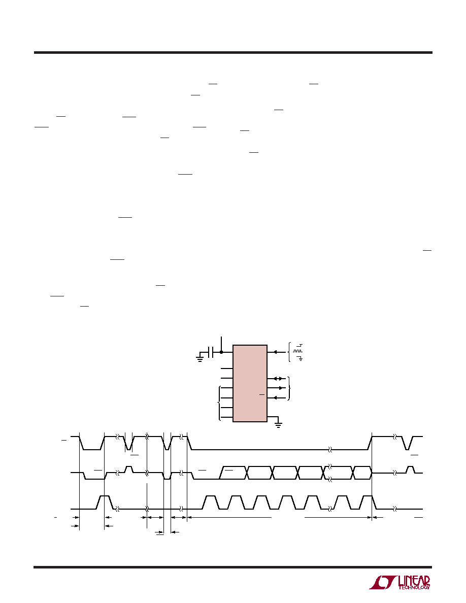
Typically, CS remains LOW during the data output state.
However, the data output state may be aborted by pulling
CS HIGH anytime between the first rising edge and the
32nd falling edge of SCK, see Figure 6. On the rising edge
of CS, the device aborts the data output state and imme-
diately initiates a new conversion. This is useful for sys-
tems not requiring all 32 bits of output data, aborting an
invalid conversion cycle or synchronizing the start of a
conversion.
External Serial Clock, 2-Wire I/O
This timing mode utilizes a 2-wire serial I/O interface. The
conversion result is shifted out of the device by an exter-
nally generated serial clock (SCK) signal, see Figure 7. CS
may be permanently tied to ground, simplifying the user
interface or isolation barrier.
The external serial clock mode is selected at the end of the
power-on reset (POR) cycle. The POR cycle is concluded
Figure 6. External Serial Clock, Reduced Data Output Length
SDO
SCK
(EXTERNAL)
CS
DATA
OUTPUT
CONVERSION
SLEEP
TEST EOC (OPTIONAL)
TEST EOC
DATA OUTPUT
Hi-Z
CONVERSION
2412 F06
MSB
SIG
CH0/CH1
BIT 8
BIT 27
BIT 9
BIT 28
BIT 29
BIT 30
EOC
BIT 31
BIT 0
EOC
Hi-Z
TEST EOC
= 50Hz REJECTION
= EXTERNAL OSCILLATOR
= 60Hz REJECTION
VCC
VCC
FO
REF+
SCK
CH1+
CH1–
SDO
GND
CS
114
2
3
13
6
7
12
8, 9, 10, 15, 16
11
REFERENCE
VOLTAGE
0.1V TO VCC
CH0+
CH0–
4
5
ANALOG INPUT RANGE
–0.5VREF TO 0.5VREF
1
F
2.7V TO 5.5V
LTC2412
3-WIRE
SPI INTERFACE
REF–
SLEEP
相关PDF资料 |
PDF描述 |
|---|---|
| SLPX222M100C7P3 | CAP ALUM 2200UF 100V 20% SNAP |
| RS3-243.3DZ/H3 | CONV DC/DC 3W 9-27VIN +/-3.3VOUT |
| AP2162MPG-13 | IC PWR SW USB 2CH 1A 8-MSOP |
| RS3-2415DZ/H3 | CONV DC/DC 3W 9-27VIN +/-15VOUT |
| SC75B-470 | INDUCTOR SMD 47UH 1.10A 2.52MHZ |
相关代理商/技术参数 |
参数描述 |
|---|---|
| DC74HC259 | 制造商:TI 制造商全称:Texas Instruments 功能描述:High Speed CMOS Logic 8-Bit Addressable Latch |
| DC-750 | 制造商:Bivar 功能描述:CARD GUIDE DEEP 7.5" 0.08" BK |
| DC-750-102 | 制造商:Bivar 功能描述:CARD GUIDE DEEP 7.5" 0.102" BK |
| DC-750-102-CI | 制造商:Bivar 功能描述:CARD GUIDE INSERT 7.5" 0.102" BK |
| DC750KA | 制造商:Dewalt 功能描述:9.6V 3/8" Cordless Compact Drill/Driver Kit 制造商:DEWALT 功能描述:9.6V DRILL/DRIVER KIT 3/8 RATCHETING CHUCK |
发布紧急采购,3分钟左右您将得到回复。