- 您现在的位置:买卖IC网 > PDF目录17066 > DC746A (Linear Technology)BOARD DELTA SIGMA ADC LTC2412 PDF资料下载
参数资料
| 型号: | DC746A |
| 厂商: | Linear Technology |
| 文件页数: | 2/36页 |
| 文件大小: | 0K |
| 描述: | BOARD DELTA SIGMA ADC LTC2412 |
| 软件下载: | QuikEval System |
| 设计资源: | DC746A Design File DC746A Schematic |
| 标准包装: | 1 |
| 系列: | QuikEval™ |
| ADC 的数量: | 1 |
| 位数: | 24 |
| 采样率(每秒): | 7.5 |
| 数据接口: | MICROWIRE?,串行,SPI? |
| 工作温度: | 0°C ~ 70°C |
| 已用 IC / 零件: | LTC2412 |
| 已供物品: | 板 |
| 相关产品: | DC590B-ND - BOARD DEMO USB SERIAL CONTROLLER LTC2412IGN#PBF-ND - IC ADC 2CH DIFF-IN 24BIT 16SSOP LTC2412IGN#TRPBF-ND - IC ADC 2CH DIFF-IN 24BIT 16SSOP LTC2412CGN#TRPBF-ND - IC ADC 2CH DIFF-IN 24BIT 16SSOP LTC2412CGN#PBF-ND - IC ADC 2CH DIFF-IN 24BIT 16SSOP LTC2412IGN#TR-ND - IC CONV A/D 24B 2CH DIFF 16-SSOP LTC2412CGN#TR-ND - IC CONV A/D 24B 2CH DIFF 16-SSOP LTC2412IGN-ND - IC CONV A/D 24B 2CH DIFF 16-SSOP LTC2412CGN-ND - IC ADC 2CH DIFF-IN 24BIT 16SSOP |
第1页当前第2页第3页第4页第5页第6页第7页第8页第9页第10页第11页第12页第13页第14页第15页第16页第17页第18页第19页第20页第21页第22页第23页第24页第25页第26页第27页第28页第29页第30页第31页第32页第33页第34页第35页第36页
LTC2412
10
2412f
VCC (Pin 1): Positive Supply Voltage. Bypass to GND with
a 10
F tantalum capacitor in parallel with 0.1F ceramic
capacitor as close to the part as possible.
REF+ (Pin 2), REF– (Pin 3): Differential Reference Input.
The voltage on these pins can have any value between GND
and VCC as long as the reference positive input, REF+, is
maintained more positive than the reference negative
input, REF –, by at least 0.1V.
CH0+ (Pin 4): Positive Input for Differential Channel 0.
CH0– (Pin 5): Negative Input for Differential Channel 0.
CH1+ (Pin 6): Positive Input for Differential Channel 1.
CH1– (Pin 7): Negative Input for Differential Channel 1.
The voltage on these four analog inputs (Pins 4 to 7) can
have any value between GND and VCC. Within these limits
the converter bipolar input range (VIN = IN+ – IN–) extends
from – 0.5 (VREF) to 0.5 (VREF). Outside this input range
the converter produces unique overrange and underrange
output codes.
GND (Pins 8, 9, 10, 15, 16): Ground. Multiple ground pins
internally connected for optimum ground current flow and
VCC decoupling. Connect each one of these pins to a ground
planethroughalowimpedanceconnection.Allfive pinsmust
be connected to ground for proper operation.
CS (Pin 11): Active LOW Digital Input. A LOW on this pin
enables the SDO digital output and wakes up the ADC.
Following each conversion the ADC automatically enters
the Sleep mode and remains in this low power state as
long as CS is HIGH. A LOW-to-HIGH transition on CS
during the Data Output transfer aborts the data transfer
and starts a new conversion.
SDO (Pin 12): Three-State Digital Output. During the Data
Output period, this pin is used as serial data output. When
the chip select CS is HIGH (CS = VCC) the SDO pin is in a
high impedance state. During the Conversion and Sleep
periods, this pin is used as the conversion status output.
The conversion status can be observed by pulling CS LOW.
SCK (Pin 13): Bidirectional Digital Clock Pin. In Internal
Serial Clock Operation mode, SCK is used as digital output
for the internal serial interface clock during the Data
Output period. In External Serial Clock Operation mode,
SCK is used as digital input for the external serial interface
clock during the Data Output period. A weak internal pull-
up is automatically activated in Internal Serial Clock Op-
eration mode. The Serial Clock Operation mode is deter-
mined by the logic level applied to the SCK pin at power up
or during the most recent falling edge of CS.
PI FU CTIO S
UU
U
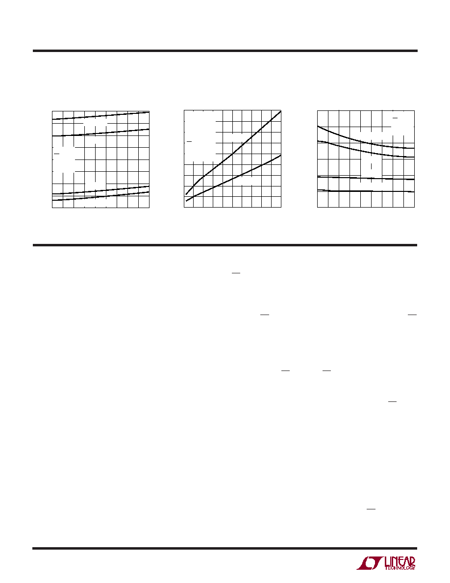
TYPICAL PERFOR A CE CHARACTERISTICS
UW
TEMPERATURE (
°C)
–45
0
SLEEP
MODE
CURRENT
(
A)
1
3
4
5
–15
15
30
90
2412 G39
2
–30
0
45
60
75
6
VCC = 5.5V
VCC = 2.7V
VCC = 5V
VCC = 3V
FO = GND
CS = VCC
SCK = NC
SDO = NC
Sleep Mode Current
vs Temperature
OUTPUT DATA RATE (READINGS/SEC)
0
100
SUPPLY
CURRENT
(
A)
200
400
500
600
60 70 80 90
1000
2412 G38
300
10 20 30 40 50
100
700
800
900
VREF = VCC
IN+ = GND
IN– = GND
SCK = NC
SDO = NC
CS = GND
FO = EXT OSC
TA = 25°C
VCC = 5V
VCC = 3V
TEMPERATURE (
°C)
–45
CONVERSION
CURRENT
(
A)
200
210
220
75
2412 G37
190
180
160
–15
15
45
–30
90
0
30
60
170
240
230
VCC = 5.5V
VCC = 2.7V
VCC = 3V
VCC = 5V
FO = GND
CS = GND
SCK = NC
SDO = NC
Conversion Current
vs Output Data Rate
Conversion Current
vs Temperature
相关PDF资料 |
PDF描述 |
|---|---|
| SLPX222M100C7P3 | CAP ALUM 2200UF 100V 20% SNAP |
| RS3-243.3DZ/H3 | CONV DC/DC 3W 9-27VIN +/-3.3VOUT |
| AP2162MPG-13 | IC PWR SW USB 2CH 1A 8-MSOP |
| RS3-2415DZ/H3 | CONV DC/DC 3W 9-27VIN +/-15VOUT |
| SC75B-470 | INDUCTOR SMD 47UH 1.10A 2.52MHZ |
相关代理商/技术参数 |
参数描述 |
|---|---|
| DC74HC259 | 制造商:TI 制造商全称:Texas Instruments 功能描述:High Speed CMOS Logic 8-Bit Addressable Latch |
| DC-750 | 制造商:Bivar 功能描述:CARD GUIDE DEEP 7.5" 0.08" BK |
| DC-750-102 | 制造商:Bivar 功能描述:CARD GUIDE DEEP 7.5" 0.102" BK |
| DC-750-102-CI | 制造商:Bivar 功能描述:CARD GUIDE INSERT 7.5" 0.102" BK |
| DC750KA | 制造商:Dewalt 功能描述:9.6V 3/8" Cordless Compact Drill/Driver Kit 制造商:DEWALT 功能描述:9.6V DRILL/DRIVER KIT 3/8 RATCHETING CHUCK |
发布紧急采购,3分钟左右您将得到回复。