- 您现在的位置:买卖IC网 > PDF目录17066 > DC746A (Linear Technology)BOARD DELTA SIGMA ADC LTC2412 PDF资料下载
参数资料
| 型号: | DC746A |
| 厂商: | Linear Technology |
| 文件页数: | 19/36页 |
| 文件大小: | 0K |
| 描述: | BOARD DELTA SIGMA ADC LTC2412 |
| 软件下载: | QuikEval System |
| 设计资源: | DC746A Design File DC746A Schematic |
| 标准包装: | 1 |
| 系列: | QuikEval™ |
| ADC 的数量: | 1 |
| 位数: | 24 |
| 采样率(每秒): | 7.5 |
| 数据接口: | MICROWIRE?,串行,SPI? |
| 工作温度: | 0°C ~ 70°C |
| 已用 IC / 零件: | LTC2412 |
| 已供物品: | 板 |
| 相关产品: | DC590B-ND - BOARD DEMO USB SERIAL CONTROLLER LTC2412IGN#PBF-ND - IC ADC 2CH DIFF-IN 24BIT 16SSOP LTC2412IGN#TRPBF-ND - IC ADC 2CH DIFF-IN 24BIT 16SSOP LTC2412CGN#TRPBF-ND - IC ADC 2CH DIFF-IN 24BIT 16SSOP LTC2412CGN#PBF-ND - IC ADC 2CH DIFF-IN 24BIT 16SSOP LTC2412IGN#TR-ND - IC CONV A/D 24B 2CH DIFF 16-SSOP LTC2412CGN#TR-ND - IC CONV A/D 24B 2CH DIFF 16-SSOP LTC2412IGN-ND - IC CONV A/D 24B 2CH DIFF 16-SSOP LTC2412CGN-ND - IC ADC 2CH DIFF-IN 24BIT 16SSOP |
第1页第2页第3页第4页第5页第6页第7页第8页第9页第10页第11页第12页第13页第14页第15页第16页第17页第18页当前第19页第20页第21页第22页第23页第24页第25页第26页第27页第28页第29页第30页第31页第32页第33页第34页第35页第36页
LTC2412
26
2412f
APPLICATIO S I FOR ATIO
WU
U
various values of source resistance imbalance between
the IN+ and IN– pins when large CIN values are used.
If possible, it is desirable to operate with the input signal
common mode voltage very close to the reference signal
common mode voltage as is the case in the ratiometric
measurement of a symmetric bridge. This configuration
eliminates the offset error caused by mismatched source
impedances.
The magnitude of the dynamic input current depends upon
the size of the very stable internal sampling capacitors and
upon the accuracy of the converter sampling clock. The
accuracy of the internal clock over the entire temperature
and power supply range is typical better than 0.5%. Such
a specification can also be easily achieved by an external
clock. When relatively stable resistors (50ppm/
°C) are
used for the external source impedance seen by IN+ and
IN–, the expected drift of the dynamic current, offset and
gain errors will be insignificant (about 1% of their respec-
tive values over the entire temperature and voltage range).
Even for the most stringent applications, a one-time
calibration operation may be sufficient.
In addition to the input sampling charge, the input ESD
protection diodes have a temperature dependent leakage
current. This current, nominally 1nA (
±10nA max), results
in a small offset shift. A 100
source resistance will create
a 0.1
V typical and 1V maximum offset voltage.
Reference Current
In a similar fashion, the LTC2412 samples the differential
reference pins REF+ and REF– transfering small amount of
charge to and from the external driving circuits thus
producing a dynamic reference current. This current does
not change the converter offset, but it may degrade the
gain and INL performance. The effect of this current can be
analyzed in the same two distinct situations.
For relatively small values of the external reference capaci-
tors (CREF < 0.01F), the voltage on the sampling capacitor
settles almost completely and relatively large values for
the source impedance result in only small errors. Such
values for CREF will deteriorate the converter offset and
gain performance without significant benefits of reference
filtering and the user is advised to avoid them.
Larger values of reference capacitors (CREF > 0.01F) may
be required as reference filters in certain configurations.
Such capacitors will average the reference sampling charge
and the external source resistance will see a quasi con-
stant reference differential impedance. When FO = LOW
(internal oscillator and 60Hz notch), the typical differential
reference resistance is 1.3M
which will generate a gain
error of approximately 0.38ppm at full-scale for each ohm
of source resistance driving REF+ or REF–. When FO =
HIGH (internal oscillator and 50Hz notch), the typical
differential reference resistance is 1.56M
which will
generate a gain error of approximately 0.32ppm at full-
scale for each ohm of source resistance driving REF+ or
REF–. When FO is driven by an external oscillator with a
frequency fEOSC (external conversion clock operation), the
typical differential reference resistance is 0.20 1012/
fEOSC and each ohm of source resistance drving REF+ or
REF– will result in 2.47 10–6 fEOSCppm gain error at full-
scale. The effect of the source resistance on the two
reference pins is additive with respect to this gain error.
The typical +FS and –FS errors for various combinations
of source resistance seen by the REF+ and REF– pins and
external capacitance CREF connected to these pins are
shown in Figures 18, 19, 20 and 21.
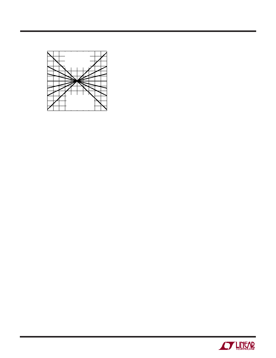
Figure 17. Offset Error vs Common Mode Voltage
(VINCM = IN+ = IN–) and Input Source Resistance
Imbalance (
RIN = RSOURCEIN+ – RSOURCEIN–) for
Large CIN Values (CIN ≥ 1F)
VINCM (V)
0
0.5
1
1.5
2
2.5
3
3.5
4
4.5
5
OFFSET
ERROR
(ppm
OF
V
REF
)
2412 F17
120
100
80
60
40
20
0
–20
–40
–60
–80
–100
–120
FO = GND
TA = 25°C
RSOURCEIN– = 500
CIN = 10F
VCC = 5V
REF+ = 5V
REF – = GND
IN+ = IN– = VINCM
A:
RIN = +400
B:
RIN = +200
C:
RIN = +100
D:
RIN = 0
E:
RIN = –100
F:
RIN = –200
G:
RIN = –400
A
B
C
D
E
F
G
相关PDF资料 |
PDF描述 |
|---|---|
| SLPX222M100C7P3 | CAP ALUM 2200UF 100V 20% SNAP |
| RS3-243.3DZ/H3 | CONV DC/DC 3W 9-27VIN +/-3.3VOUT |
| AP2162MPG-13 | IC PWR SW USB 2CH 1A 8-MSOP |
| RS3-2415DZ/H3 | CONV DC/DC 3W 9-27VIN +/-15VOUT |
| SC75B-470 | INDUCTOR SMD 47UH 1.10A 2.52MHZ |
相关代理商/技术参数 |
参数描述 |
|---|---|
| DC74HC259 | 制造商:TI 制造商全称:Texas Instruments 功能描述:High Speed CMOS Logic 8-Bit Addressable Latch |
| DC-750 | 制造商:Bivar 功能描述:CARD GUIDE DEEP 7.5" 0.08" BK |
| DC-750-102 | 制造商:Bivar 功能描述:CARD GUIDE DEEP 7.5" 0.102" BK |
| DC-750-102-CI | 制造商:Bivar 功能描述:CARD GUIDE INSERT 7.5" 0.102" BK |
| DC750KA | 制造商:Dewalt 功能描述:9.6V 3/8" Cordless Compact Drill/Driver Kit 制造商:DEWALT 功能描述:9.6V DRILL/DRIVER KIT 3/8 RATCHETING CHUCK |
发布紧急采购,3分钟左右您将得到回复。