- 您现在的位置:买卖IC网 > PDF目录17066 > DC746A (Linear Technology)BOARD DELTA SIGMA ADC LTC2412 PDF资料下载
参数资料
| 型号: | DC746A |
| 厂商: | Linear Technology |
| 文件页数: | 9/36页 |
| 文件大小: | 0K |
| 描述: | BOARD DELTA SIGMA ADC LTC2412 |
| 软件下载: | QuikEval System |
| 设计资源: | DC746A Design File DC746A Schematic |
| 标准包装: | 1 |
| 系列: | QuikEval™ |
| ADC 的数量: | 1 |
| 位数: | 24 |
| 采样率(每秒): | 7.5 |
| 数据接口: | MICROWIRE?,串行,SPI? |
| 工作温度: | 0°C ~ 70°C |
| 已用 IC / 零件: | LTC2412 |
| 已供物品: | 板 |
| 相关产品: | DC590B-ND - BOARD DEMO USB SERIAL CONTROLLER LTC2412IGN#PBF-ND - IC ADC 2CH DIFF-IN 24BIT 16SSOP LTC2412IGN#TRPBF-ND - IC ADC 2CH DIFF-IN 24BIT 16SSOP LTC2412CGN#TRPBF-ND - IC ADC 2CH DIFF-IN 24BIT 16SSOP LTC2412CGN#PBF-ND - IC ADC 2CH DIFF-IN 24BIT 16SSOP LTC2412IGN#TR-ND - IC CONV A/D 24B 2CH DIFF 16-SSOP LTC2412CGN#TR-ND - IC CONV A/D 24B 2CH DIFF 16-SSOP LTC2412IGN-ND - IC CONV A/D 24B 2CH DIFF 16-SSOP LTC2412CGN-ND - IC ADC 2CH DIFF-IN 24BIT 16SSOP |
第1页第2页第3页第4页第5页第6页第7页第8页当前第9页第10页第11页第12页第13页第14页第15页第16页第17页第18页第19页第20页第21页第22页第23页第24页第25页第26页第27页第28页第29页第30页第31页第32页第33页第34页第35页第36页
LTC2412
17
2412f
APPLICATIO S I FOR ATIO
WU
U
anytime a LOW-to-HIGH transition is detected at the CS
pin after the converter has entered the data output state
(i.e., after the first rising edge of SCK occurs with
CS = LOW).
Finally, CS can be used to control the free-running modes
of operation, see Serial Interface Timing Modes section.
Grounding CS will force the ADC to continuously convert
at the maximum output rate selected by FO.
SERIAL INTERFACE TIMING MODES
The LTC2412’s 3-wire interface is SPI and MICROWIRE
compatible. This interface offers several flexible modes of
operation. These include internal/external serial clock,
2- or 3-wire I/O, single cycle conversion and autostart. The
following sections describe each of these serial interface
timing modes in detail. In all these cases, the converter
can use the internal oscillator (FO = LOW or FO = HIGH) or
an external oscillator connected to the FO pin. Refer to
Table 4 for a summary.
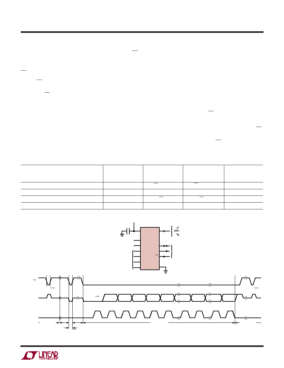
External Serial Clock, Single Cycle Operation
(SPI/MICROWIRE Compatible)
This timing mode uses an external serial clock to shift out
the conversion result and a CS signal to monitor and
control the state of the conversion cycle, see Figure 5.
The serial clock mode is selected on the falling edge of CS.
To select the external serial clock mode, the serial clock pin
(SCK) must be LOW during each CS falling edge.
Figure 5. External Serial Clock, Single Cycle Operation
Table 4. LTC2412 Interface Timing Modes
Conversion
Data
Connection
SCK
Cycle
Output
and
Configuration
Source
Control
Waveforms
External SCK, Single Cycle Conversion
External
CS and SCK
Figures 5, 6
External SCK, 2-Wire I/O
External
SCK
Figure 7
Internal SCK, Single Cycle Conversion
Internal
CS
↓
CS
↓
Figures 8, 9
Internal SCK, 2-Wire I/O, Continuous Conversion
Internal
Continuous
Internal
Figure 10
EOC
BIT 31
SDO
SCK
(EXTERNAL)
CS
TEST EOC
SUB LSB
MSB
SIG
CH0/CH1
BIT 0
LSB
BIT 5
BIT 27
BIT 26
BIT 28
BIT 29
BIT 30
SLEEP
TEST EOC
(OPTIONAL)
DATA OUTPUT
CONVERSION
2412 F05
CONVERSION
Hi-Z
TEST EOC
= 50Hz REJECTION
= EXTERNAL OSCILLATOR
= 60Hz REJECTION
VCC
VCC
FO
REF+
SCK
CH1+
CH1–
SDO
GND
CS
114
2
3
13
6
7
12
8, 9, 10, 15, 16
11
REFERENCE
VOLTAGE
0.1V TO VCC
CH0+
CH0–
4
5
ANALOG INPUT RANGE
–0.5VREF TO 0.5VREF
1
F
2.7V TO 5.5V
LTC2412
3-WIRE
SPI INTERFACE
REF–
相关PDF资料 |
PDF描述 |
|---|---|
| SLPX222M100C7P3 | CAP ALUM 2200UF 100V 20% SNAP |
| RS3-243.3DZ/H3 | CONV DC/DC 3W 9-27VIN +/-3.3VOUT |
| AP2162MPG-13 | IC PWR SW USB 2CH 1A 8-MSOP |
| RS3-2415DZ/H3 | CONV DC/DC 3W 9-27VIN +/-15VOUT |
| SC75B-470 | INDUCTOR SMD 47UH 1.10A 2.52MHZ |
相关代理商/技术参数 |
参数描述 |
|---|---|
| DC74HC259 | 制造商:TI 制造商全称:Texas Instruments 功能描述:High Speed CMOS Logic 8-Bit Addressable Latch |
| DC-750 | 制造商:Bivar 功能描述:CARD GUIDE DEEP 7.5" 0.08" BK |
| DC-750-102 | 制造商:Bivar 功能描述:CARD GUIDE DEEP 7.5" 0.102" BK |
| DC-750-102-CI | 制造商:Bivar 功能描述:CARD GUIDE INSERT 7.5" 0.102" BK |
| DC750KA | 制造商:Dewalt 功能描述:9.6V 3/8" Cordless Compact Drill/Driver Kit 制造商:DEWALT 功能描述:9.6V DRILL/DRIVER KIT 3/8 RATCHETING CHUCK |
发布紧急采购,3分钟左右您将得到回复。