- 您现在的位置:买卖IC网 > PDF目录17066 > DC746A (Linear Technology)BOARD DELTA SIGMA ADC LTC2412 PDF资料下载
参数资料
| 型号: | DC746A |
| 厂商: | Linear Technology |
| 文件页数: | 18/36页 |
| 文件大小: | 0K |
| 描述: | BOARD DELTA SIGMA ADC LTC2412 |
| 软件下载: | QuikEval System |
| 设计资源: | DC746A Design File DC746A Schematic |
| 标准包装: | 1 |
| 系列: | QuikEval™ |
| ADC 的数量: | 1 |
| 位数: | 24 |
| 采样率(每秒): | 7.5 |
| 数据接口: | MICROWIRE?,串行,SPI? |
| 工作温度: | 0°C ~ 70°C |
| 已用 IC / 零件: | LTC2412 |
| 已供物品: | 板 |
| 相关产品: | DC590B-ND - BOARD DEMO USB SERIAL CONTROLLER LTC2412IGN#PBF-ND - IC ADC 2CH DIFF-IN 24BIT 16SSOP LTC2412IGN#TRPBF-ND - IC ADC 2CH DIFF-IN 24BIT 16SSOP LTC2412CGN#TRPBF-ND - IC ADC 2CH DIFF-IN 24BIT 16SSOP LTC2412CGN#PBF-ND - IC ADC 2CH DIFF-IN 24BIT 16SSOP LTC2412IGN#TR-ND - IC CONV A/D 24B 2CH DIFF 16-SSOP LTC2412CGN#TR-ND - IC CONV A/D 24B 2CH DIFF 16-SSOP LTC2412IGN-ND - IC CONV A/D 24B 2CH DIFF 16-SSOP LTC2412CGN-ND - IC ADC 2CH DIFF-IN 24BIT 16SSOP |
第1页第2页第3页第4页第5页第6页第7页第8页第9页第10页第11页第12页第13页第14页第15页第16页第17页当前第18页第19页第20页第21页第22页第23页第24页第25页第26页第27页第28页第29页第30页第31页第32页第33页第34页第35页第36页
LTC2412
25
2412f
APPLICATIO S I FOR ATIO
WU
U
of input multiplexers, wires, connectors or sensors, the
LTC2412 can maintain its exceptional accuracy while
operating with relative large values of source resistance as
shown in Figures 13 and 14. These measured results may
be slightly different from the first order approximation
suggested earlier because they include the effect of the
actual second order input network together with the non-
linear settling process of the input amplifiers. For small CIN
values, the settling on IN+ and IN– occurs almost indepen-
dently and there is little benefit in trying to match the
source impedance for the two pins.
Larger values of input capacitors (CIN > 0.01F) may be
required in certain configurations for antialiasing or gen-
eral input signal filtering. Such capacitors will average the
input sampling charge and the external source resistance
will see a quasi constant input differential impedance.
When FO = LOW (internal oscillator and 60Hz notch), the
typical differential input resistance is 1.8M
which will
generate a gain error of approximately 0.28ppm at full-
scale for each ohm of source resistance driving IN+ or IN.
When FO = HIGH (internal oscillator and 50Hz notch), the
typical differential input resistance is 2.16M
which will
generate a gain error of approximately 0.23ppm at full-
scale for each ohm of source resistance driving IN+ or IN.
When FO is driven by an external oscillator with a fre-
quency fEOSC (external conversion clock operation), the
typical differential input resistance is 0.28 1012/fEOSC
and each ohm of source resistance driving IN+ or IN– will
result in 1.78 10–6 fEOSCppm gain error at full-scale. The
effect of the source resistance on the two input pins is
additive with respect to this gain error. The typical +FS and
–FS errors as a function of the sum of the source resis-
tance seen by IN+ and IN– for large values of CIN are shown
in Figures 15 and 16.
In addition to this gain error, an offset error term may also
appear. The offset error is proportional with the mismatch
between the source impedance driving the two input pins
IN+ and IN– and with the difference between the input and
reference common mode voltages. While the input drive
circuit nonzero source impedance combined with the con-
verter average input current will not degrade the INL
performance, indirect distortion may result from the modu-
lation of the offset error by the common mode component
of the input signal. Thus, when using large CIN capacitor
values, it is advisable to carefully match the source imped-
ance seen by the IN+ and IN– pins. When FO = LOW
(internal oscillator and 60Hz notch), every 1
mismatch
in source impedance transforms a full-scale common
mode input signal into a differential mode input signal of
0.28ppm. When FO = HIGH (internal oscillator and 50Hz
notch), every 1
mismatch in source impedance trans-
forms a full-scale common mode input signal into a differ-
ential mode input signal of 0.23ppm. When FO is driven by
an external oscillator with a frequency fEOSC, every 1
mismatch in source impedance transforms a full-scale
common mode input signal into a differential mode input
signal of 1.78 10–6 fEOSCppm. Figure 17 shows the
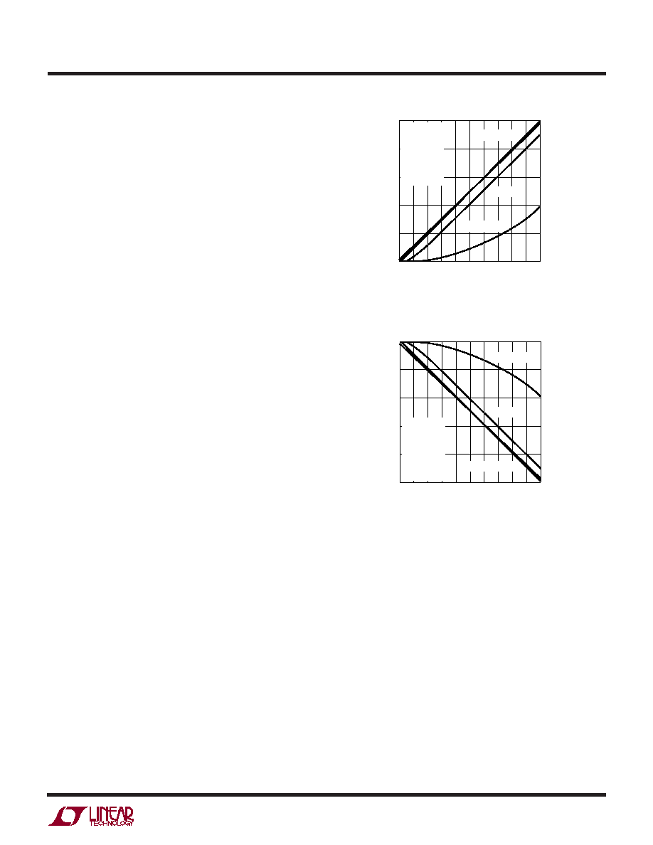
typical offset error due to input common mode voltage for
Figure 15. +FS Error vs RSOURCE at IN+ or IN– (Large CIN)
Figure 16. –FS Error vs RSOURCE at IN
+ or IN– (Large CIN)
RSOURCE ()
0 100 200 300 400 500 600 700 800 900 1000
+FS
ERROR
(ppm
OF
V
REF
)
2412 F15
300
240
180
120
60
0
VCC = 5V
REF+ = 5V
REF – = GND
IN+ = 3.75V
IN– = 1.25V
FO = GND
TA = 25°C
CIN = 0.01F
CIN = 0.1F
CIN = 1F, 10F
RSOURCE ()
0 100 200 300 400 500 600 700 800 900 1000
–
FS
ERROR
(ppm
OF
V
REF
)
2412 F16
0
–60
–120
–180
–240
–300
VCC = 5V
REF+ = 5V
REF – = GND
IN+ = 1.25V
IN– = 3.75V
FO = GND
TA = 25°C
CIN = 0.01F
CIN = 0.1F
CIN = 1F, 10F
相关PDF资料 |
PDF描述 |
|---|---|
| SLPX222M100C7P3 | CAP ALUM 2200UF 100V 20% SNAP |
| RS3-243.3DZ/H3 | CONV DC/DC 3W 9-27VIN +/-3.3VOUT |
| AP2162MPG-13 | IC PWR SW USB 2CH 1A 8-MSOP |
| RS3-2415DZ/H3 | CONV DC/DC 3W 9-27VIN +/-15VOUT |
| SC75B-470 | INDUCTOR SMD 47UH 1.10A 2.52MHZ |
相关代理商/技术参数 |
参数描述 |
|---|---|
| DC74HC259 | 制造商:TI 制造商全称:Texas Instruments 功能描述:High Speed CMOS Logic 8-Bit Addressable Latch |
| DC-750 | 制造商:Bivar 功能描述:CARD GUIDE DEEP 7.5" 0.08" BK |
| DC-750-102 | 制造商:Bivar 功能描述:CARD GUIDE DEEP 7.5" 0.102" BK |
| DC-750-102-CI | 制造商:Bivar 功能描述:CARD GUIDE INSERT 7.5" 0.102" BK |
| DC750KA | 制造商:Dewalt 功能描述:9.6V 3/8" Cordless Compact Drill/Driver Kit 制造商:DEWALT 功能描述:9.6V DRILL/DRIVER KIT 3/8 RATCHETING CHUCK |
发布紧急采购,3分钟左右您将得到回复。