- 您现在的位置:买卖IC网 > PDF目录16128 > DMA-MC-O4-N2 (Lattice Semiconductor Corporation)IP CORE MCDMA CTLR ORCA 4 PDF资料下载
参数资料
| 型号: | DMA-MC-O4-N2 |
| 厂商: | Lattice Semiconductor Corporation |
| 文件页数: | 4/28页 |
| 文件大小: | 0K |
| 描述: | IP CORE MCDMA CTLR ORCA 4 |
| 标准包装: | 1 |
| 系列: | * |
| 其它名称: | DMAMCO4N2 |
第1页第2页第3页当前第4页第5页第6页第7页第8页第9页第10页第11页第12页第13页第14页第15页第16页第17页第18页第19页第20页第21页第22页第23页第24页第25页第26页第27页第28页
�� �
�
�Lattice� Semiconductor�
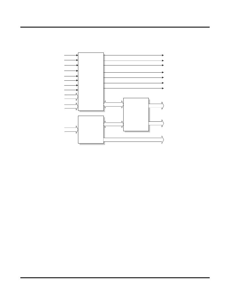
�Block� Diagram�
�Figure� 1� shows� the� block� diagram� of� this� core.�
�Figure� 1.� Block� Diagram� of� MCDMA� Core�
�cs_n�
�eopin_n�
�reset�
�clk�
�Multi-Channel� DMA� Controller� User’s� Guide�
�hreq�
�aen�
�iorout_n�
�iowout_n�
�iorin_n�
�iowin_n�
�ready�
�hlda�
�ain[AIN_BUS_WIDTH-1:0]�
�dbin[DATA_BUS_WIDTH-1:0]�
�dreq[N-1:0]�
�CPU� Interface�
�and�
�DMA� State�
�Machine�
�Priority�
�Request�
�Register�
�Block�
�memr_n�
�memw_n�
�eopout_n�
�aout[ADDR_BUS_WIDTH-1:0]�
�dbout[DATA_BUS_WIDTH-1:0]�
�Encoder�
�dack[N-1:0]�
�N� =� Number� of� channels�
�Functional� Description�
�The� MCDMA� contains� three� basic� blocks� of� control� logic:� CPU� Interface� (Data� and� Control� Blocks),� the� DMA� State�
�Machine,� and� the� Priority� Request� Encoder�
�CPU� Interface� Control�
�This� explanation� applies� mainly� to� the� non-8237� mode� because� most� of� the� programmability� lies� in� this� mode.� How-�
�ever,� the� concepts� are� also� applicable� to� the� 8237� mode.�
�The� CPU� Interface� Control� block� ?rst� decodes� the� ain� bus.� It� then� generates� the� enable� signals� to� the� selected�
�registers� or� to� a� subset� of� the� selected� registers� when� byte� enables� are� present� during� the� write� cycle.� When� the�
�registers� are� read,� it� provides� a� select� signal� to� the� multiplexer� that� routes� the� appropriate� register� contents� onto�
�the� data� bus.�
�CPU� Interface� Data�
�The� CPU� Interface� Data� block� contains� all� the� con?guration� registers.� It� includes� all� the� routing� logic� required� to�
�transfer� either� the� selected� register’s� contents� (during� the� register� read� cycle)� or� the� temporary� register� contents�
�(during� the� memory� write� cycle� of� a� memory-to-memory� transfer).�
�DMA� Finite� State� Machine�
�The� DMA� FSM� (Finite� State� Machine)� module� initiates� data� transfers� and� generates� control� signals� for� various�
�transfer� modes.� It� also� generates� the� address� and� address-enable� signals� (� aen� ).� The� FSM� exchanges� signals� with�
�the� CPU� interface� block� and� priority� encoder� block.� The� state� machine� in� the� 8237� mode� is� similar� to� the� non-8237�
�mode� except� a� few� additional� FSM� branches� in� 8237� mode� that� incorporate:�
�4�
�相关PDF资料 |
PDF描述 |
|---|---|
| LHL10TB220K | INDUCTOR 22UH 2.1A RADIAL |
| EBC31DRTH | CONN EDGECARD 62POS DIP .100 SLD |
| LHL10TB183J | INDUCTOR 18000UH 81MA RADIAL |
| LHL10TB182J | INDUCTOR 1800UH .29A RADIAL |
| 1487EK | WIREWAY BOX CONNECTOR 8X8" |
相关代理商/技术参数 |
参数描述 |
|---|---|
| DMA-MC-SC-N3 | 功能描述:数字信号处理器和控制器 - DSP, DSC DMA Controller RoHS:否 制造商:Microchip Technology 核心:dsPIC 数据总线宽度:16 bit 程序存储器大小:16 KB 数据 RAM 大小:2 KB 最大时钟频率:40 MHz 可编程输入/输出端数量:35 定时器数量:3 设备每秒兆指令数:50 MIPs 工作电源电压:3.3 V 最大工作温度:+ 85 C 封装 / 箱体:TQFP-44 安装风格:SMD/SMT |
| DMA-MC-XM-N3 | 功能描述:数字信号处理器和控制器 - DSP, DSC DMA Controller RoHS:否 制造商:Microchip Technology 核心:dsPIC 数据总线宽度:16 bit 程序存储器大小:16 KB 数据 RAM 大小:2 KB 最大时钟频率:40 MHz 可编程输入/输出端数量:35 定时器数量:3 设备每秒兆指令数:50 MIPs 工作电源电压:3.3 V 最大工作温度:+ 85 C 封装 / 箱体:TQFP-44 安装风格:SMD/SMT |
| DMA-MC-XP-N2 | 功能描述:数字信号处理器和控制器 - DSP, DSC DMA Controller RoHS:否 制造商:Microchip Technology 核心:dsPIC 数据总线宽度:16 bit 程序存储器大小:16 KB 数据 RAM 大小:2 KB 最大时钟频率:40 MHz 可编程输入/输出端数量:35 定时器数量:3 设备每秒兆指令数:50 MIPs 工作电源电压:3.3 V 最大工作温度:+ 85 C 封装 / 箱体:TQFP-44 安装风格:SMD/SMT |
| DM-A-PP | 制造商:DDK 制造商全称:DDK Ltd. 功能描述:Conversion Connector |
| DMA-SG-E3-U1 | 功能描述:开发软件 DMA Scatter/Gather RoHS:否 制造商:Atollic Inc. 产品:Compilers/Debuggers 用于:ARM7, ARM9, Cortex-A, Cortex-M, Cortex-R Processors |
发布紧急采购,3分钟左右您将得到回复。