- 您现在的位置:买卖IC网 > Datasheet目录406 > DMN32D2LV-7 (Diodes Inc)MOSFET N-CH DUAL 30V SOT-563 Datasheet资料下载
参数资料
| 型号: | DMN32D2LV-7 |
| 厂商: | Diodes Inc |
| 文件页数: | 2/6页 |
| 文件大小: | 0K |
| 描述: | MOSFET N-CH DUAL 30V SOT-563 |
| 产品变化通告: | Bond Wire Change 11/Nov/2011 |
| 标准包装: | 1 |
| FET 型: | 2 个 N 沟道(双) |
| FET 特点: | 逻辑电平门 |
| 漏极至源极电压(Vdss): | 30V |
| 电流 - 连续漏极(Id) @ 25° C: | 400mA |
| 开态Rds(最大)@ Id, Vgs @ 25° C: | 1.2 欧姆 @ 100mA,4V |
| Id 时的 Vgs(th)(最大): | 1.2V @ 250µA |
| 输入电容 (Ciss) @ Vds: | 39pF @ 3V |
| 功率 - 最大: | 400mW |
| 安装类型: | 表面贴装 |
| 封装/外壳: | SOT-563,SOT-666 |
| 供应商设备封装: | SOT-563 |
| 包装: | 标准包装 |
| 其它名称: | DMN32D2LV-7DIDKR |
�� �
�
�DMN32D2LV�
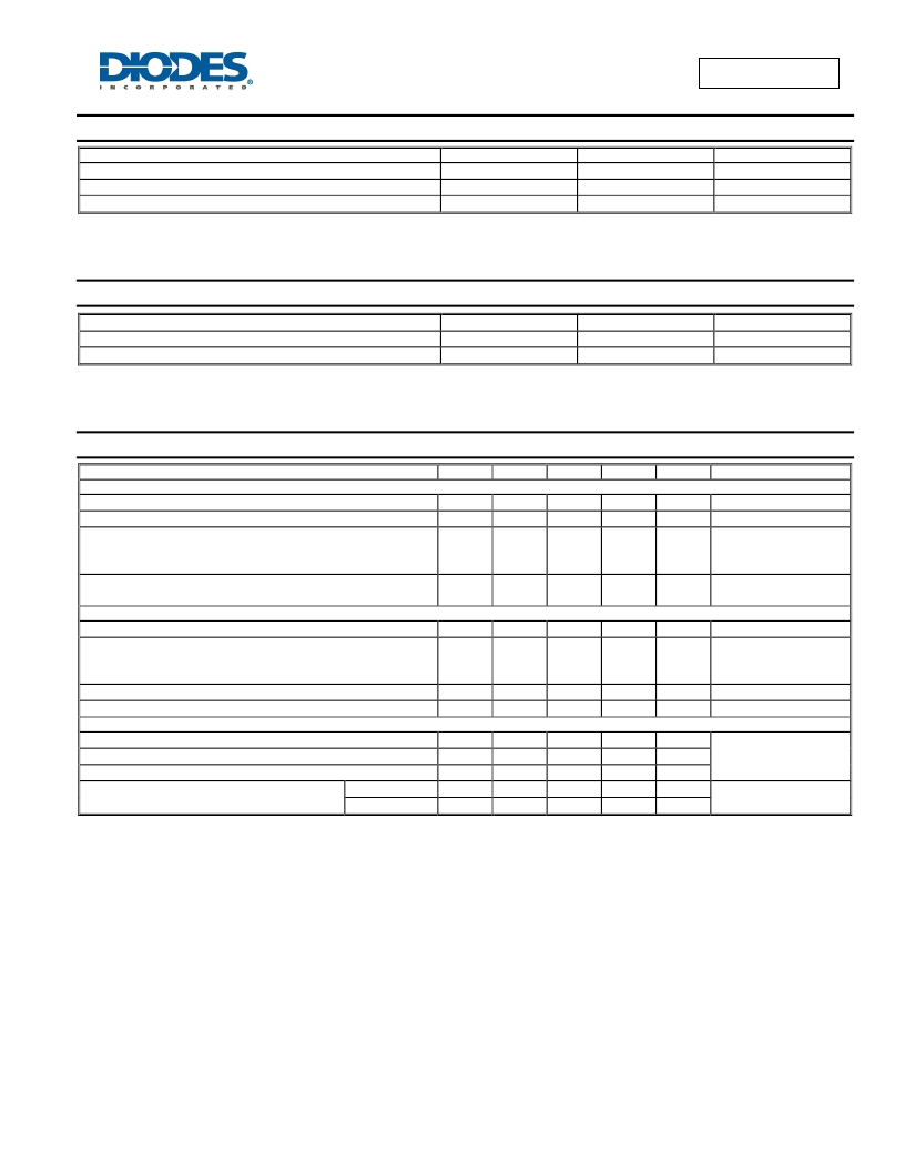
�Maximum� Ratings�
�(@T� A� =� +25°C,� unless� otherwise� specified.)�
�Drain� Source� Voltage�
�Gate-Source� Voltage�
�Drain� Current� (Note� 5)�
�Characteristic�
�Symbol�
�V� DSS�
�V� GSS�
�I� D�
�Value�
�30�
�?� 10�
�400�
�Unit�
�V�
�V�
�mA�
�Thermal� Characteristics�
�(@T� A� =� +25°C,� unless� otherwise� specified.)�
�Total� Power� Dissipation� (Note� 5)�
�Thermal� Resistance,� Junction� to� Ambient� (Note� 5)�
�Operating� and� Storage� Temperature� Range�
�P� D�
�R� θ� JA�
�T� J� ,� T� STG�
�400�
�313�
�-55� to� +150�
�mW�
�?� C/W�
�?� C�
�Electrical� Characteristics�
�(@T� A� =� +25°C,� unless� otherwise� specified.)�
�Characteristic�
�Symbol�
�Min�
�Typ�
�Max�
�Unit�
�Test� Condition�
�OFF� CHARACTERISTICS� (Note� 6)�
�Drain-Source� Breakdown� Voltage�
�BV� DSS�
�30�
�?�
�?�
�V�
�V� GS� =� 0V,� I� D� =� 250� μ� A�
�Zero� Gate� Voltage� Drain� Current�
�Gate-Body� Leakage�
�Gate-Body� Leakage� (Note� 7)�
�@� T� J� =� +25°C�
�@� T� J� =� +25°C�
�@� T� J� =� +105°C�
�@� T� J� =� +125°C�
�I� DSS�
�I� GSS�
�I� GSS�
�?�
�?�
�?�
�?�
�??�
�??�
�?� 1�
�?� 8�
�?� 15�
�1�
�?� 10�
�?� 500�
�?� 100�
�?� 100�
�?� 100�
�?� A�
�?� A�
�nA�
�nA�
�nA�
�nA�
�V� DS� =� 30V,� V� GS� =� 0V�
�V� GS� =� ±10V,� V� DS� =� 0V�
�V� GS� =� ±5V,� V� DS� =� 0V�
�V� GS� =� ±2.5V,� V� DS� =� 0V�
�V� GS� =� ±2.5V,� V� DS� =� 0V�
�ON� CHARACTERISTICS� (Note� 6)�
�Gate� Threshold� Voltage�
�Static� Drain-Source� On-Resistance�
�Forward� Transconductance�
�Source-Drain� Diode� Forward� Voltage�
�V� GS(th)�
�R� DS� (ON)�
�|Y� fs� |�
�V� SD�
�0.6�
�??�
�??�
�?�
�100�
�0.5�
�?�
�??�
�??�
�?�
�?�
�?�
�1.2�
�2.2�
�1.5�
�1.2�
�?�
�1.4�
�V�
�?�
�mS�
�V�
�V� DS� =� V� GS� ,� I� D� =� 250� μ� A�
�V� GS� =� 1.8V,� I� D� =� 20mA�
�V� GS� =� 2.5V,� I� D� =� 20mA�
�V� GS� =� 4.0V,� I� D� =� 100mA�
�V� DS� =10V,� I� D� =� 0.1A�
�V� GS� =� 0V,� I� S� =� 115mA�
�DYNAMIC� CHARACTERISTICS� (Note� 7)�
�Input� Capacitance�
�Output� Capacitance�
�Reverse� Transfer� Capacitance�
�C� iss�
�C� oss�
�C� rss�
�?�
�?�
�?�
�39�
�10�
�3.6�
�?�
�?�
�?�
�pF�
�pF�
�pF�
�V� DS� =� 3V,� V� GS� =� 0V�
�f� =� 1.0MHz�
�Switching� Time�
�Turn-on� Time�
�Turn-off� Time�
�t� on�
�t� off�
�??�
�??�
�11�
�51�
�??�
�??�
�nS�
�nS�
�V� DD� =� 5V,� I� D� =� 10� mA,�
�V� GS� =� 5V�
�Notes:�
�5.� Device� mounted� on� FR-4� PCB,� 1� inch� x� 0.85� inch� x� 0.062� inch;� pad� layout� as� shown� on� Diodes� Inc.� suggested� pad� layout� document� AP02001,� which� can�
�be� found� on� our� website� at� http://www.diodes.com.�
�6.� Short� duration� pulse� test� used� to� minimize� self-heating� effect.�
�7.� Guaranteed� by� design.� Not� subject� to� production� testing.�
�DMN32D2LV�
�Document� number:� DS31121� Rev.� 7� -� 2�
�2� of� 6�
�www.diodes.com�
�January� 2014�
�?� Diodes� Incorporated�
�相关PDF资料 |
PDF描述 |
|---|---|
| DMN3300U-7 | MOSFET N-CH 30V 2A SOT23-3 |
| DMN3404L-7 | MOSFET N-CH 30V 5.8A SOT-23 |
| DMN3730U-7 | MOSFET N-CH 30V 750MA SOT23 |
| DMN3730UFB-7 | MOSFET N-CH 30V 750MA DFN |
| DMN3730UFB4-7 | MOSFET N-CH 30V 750MA DFN |
相关代理商/技术参数 |
参数描述 |
|---|---|
| DMN3300U | 制造商:Diodes Incorporated 功能描述:MOSFET N CH W DIODE 30V 2A SOT23 制造商:Diodes Incorporated 功能描述:MOSFET, N CH, W DIODE, 30V, 2A, SOT23 制造商:Diodes Incorporated 功能描述:MOSFET, N CH, W DIODE, 30V, 2A, SOT23; Transistor Polarity:N Channel; Continuous Drain Current Id:2A; Drain Source Voltage Vds:30V; On Resistance Rds(on):0.1ohm; Rds(on) Test Voltage Vgs:4.5V; Power Dissipation Pd:600mW ;RoHS Compliant: Yes |
| DMN3300U-7 | 功能描述:MOSFET 600mW 30Vdss RoHS:否 制造商:STMicroelectronics 晶体管极性:N-Channel 汲极/源极击穿电压:650 V 闸/源击穿电压:25 V 漏极连续电流:130 A 电阻汲极/源极 RDS(导通):0.014 Ohms 配置:Single 最大工作温度: 安装风格:Through Hole 封装 / 箱体:Max247 封装:Tube |
| DMN3300U-7-F | 制造商:TYSEMI 制造商全称:TY Semiconductor Co., Ltd 功能描述:Product specification |
| DMN3404L | 制造商:Diodes Incorporated 功能描述: |
| DMN3404L-7 | 功能描述:MOSFET N-CHANNEL ENHANCEMENT MODE RoHS:否 制造商:STMicroelectronics 晶体管极性:N-Channel 汲极/源极击穿电压:650 V 闸/源击穿电压:25 V 漏极连续电流:130 A 电阻汲极/源极 RDS(导通):0.014 Ohms 配置:Single 最大工作温度: 安装风格:Through Hole 封装 / 箱体:Max247 封装:Tube |
发布紧急采购,3分钟左右您将得到回复。