- 您现在的位置:买卖IC网 > PDF目录4573 > DS1865T+T&R (Maxim Integrated Products)IC PON CONTROL TRI 28-TQFN PDF资料下载
参数资料
| 型号: | DS1865T+T&R |
| 厂商: | Maxim Integrated Products |
| 文件页数: | 7/67页 |
| 文件大小: | 0K |
| 描述: | IC PON CONTROL TRI 28-TQFN |
| 产品培训模块: | Lead (SnPb) Finish for COTS Obsolescence Mitigation Program |
| 标准包装: | 2,500 |
| 系列: | * |
| 类型: | * |
| 应用: | * |
| 安装类型: | 表面贴装 |
| 封装/外壳: | 28-WFQFN 裸露焊盘 |
| 供应商设备封装: | 28-TQFN-EP(5x5) |
| 包装: | 带卷 (TR) |
第1页第2页第3页第4页第5页第6页当前第7页第8页第9页第10页第11页第12页第13页第14页第15页第16页第17页第18页第19页第20页第21页第22页第23页第24页第25页第26页第27页第28页第29页第30页第31页第32页第33页第34页第35页第36页第37页第38页第39页第40页第41页第42页第43页第44页第45页第46页第47页第48页第49页第50页第51页第52页第53页第54页第55页第56页第57页第58页第59页第60页第61页第62页第63页第64页第65页第66页第67页
DS1865
PON Triplexer Control and
Monitoring Circuit
____________________________________________________________________
15
inadequate VCC exists to operate the laser driver. Once
adequate VCC is present to clear the VCC low alarm, the
outputs are enabled following the same sequence as the
power-up sequence.
As previously mentioned, the FETG is an output used to
disable the laser current through a series nMOSFET or
pMOSFET. This requires that the FETG output can sink
or source current. Because the DS1865 does not know
if it should sink or source current before VCC exceeds
VPOA, which triggers the EE recall, this output will
be high impedance when VCC is below VPOA (see the
Low-Voltage Operation section for details and
diagram). The application circuit must use a pullup or
pulldown resistor on this pin that pulls FETG to the
alarm/shutdown state (high for a pMOS, low for a
nMOS). Once VCC is above VPOA, the DS1865 pulls the
FETG output to the state determined by the FETG DIR
bit (Table 02h, Register 89h). FETG DIR is 0 if an nMOS
is used and 1 if a pMOS is used.
Determining Alarm Causes
Using the I2C Interface
To determine the cause of the TX-F or FETG alarm, the
system processor can read the DS1865’s Alarm Trap
Bytes (ATB) through the I2C interface (in Table 01h). The
ATB has a bit for each alarm. Any time an alarm occurs,
regardless of the mask bit’s state, the DS1865 sets the
corresponding bit in the ATB. Active ATB bits remain set
until written to zeros through the I2C interface. On power-
up, the ATB is zeros until alarms dictate otherwise.
Die Identification
The DS1865 has an ID hard coded to its die. Two regis-
ters (Table 02h bytes 86h–87h) are assigned for this
feature. Byte 86h reads 65h to identify the part as the
DS1865, byte 87h reads the die revision.
Low-Voltage Operation
The DS1865 contains two power-on reset (POR) levels.
The lower level is a digital POR (VPOD) and the higher
level is an analog POR (VPOA). At startup, before the
supply voltage rises above VPOA, the outputs are dis-
abled (FETG and BIAS outputs are high impedance,
MOD is low), all SRAM locations are low (including
shadowed EEPROM), and all analog circuitry is dis-
abled. When VCC reaches VPOA, the SEE is recalled,
and the analog circuitry is enabled. While VCC remains
above VPOA, the device is in its normal operating state,
and it responds based on its nonvolatile configuration.
If during operation VCC falls below VPOA but is still
above VPOD, the SRAM retains the SEE settings from
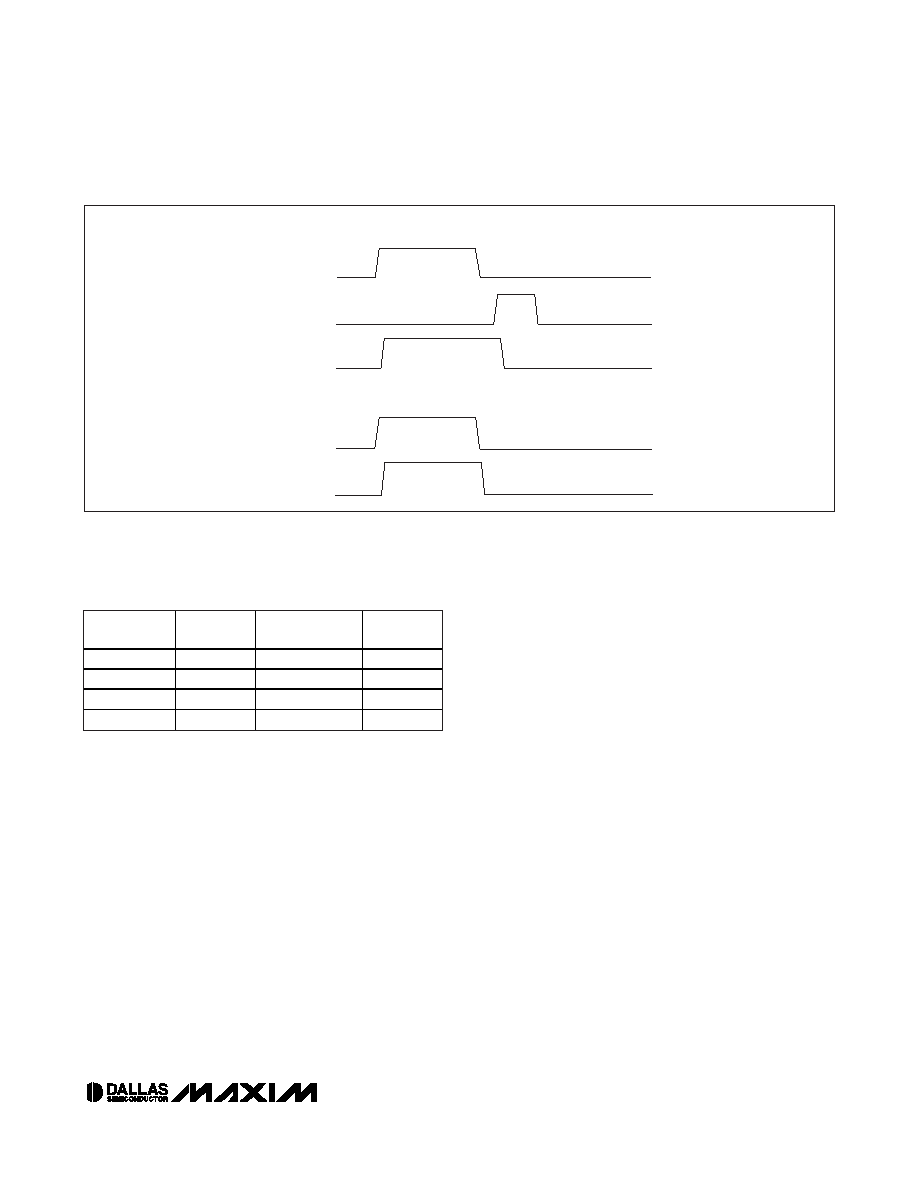
TX-F LATCHED OPERATION
TX-F NON LATCHED OPERATION
DETECTION OF
TX-F FAULT
TX-D OR
TX-F RESET
TX-F
DETECTION OF
TX-F FAULT
TX-F
Figure 5. TX-F Timing
Table 4. TX-F as a Function of TX-D and
Alarm Sources
VCC > VPOA
TX-D
NONMASKED
TX-F ALARM
TX-F
No
X
1
Yes
0
Yes
0
1
Yes
1
X
0
相关PDF资料 |
PDF描述 |
|---|---|
| TLE8264E | IC SYSTEM BASIS CHIP DSO-36 |
| MAX4507CWN+T | IC SIGNAL LINE PROTECTOR 18-SOIC |
| TLE8263-2E | IC SYSTEM BASIS CHIP DSO-36 |
| TLE8263E | IC SYSTEM BASIS CHIP DSO-36 |
| TLE8262E | IC SYSTEM BASIS CHIP DSO-36 |
相关代理商/技术参数 |
参数描述 |
|---|---|
| DS1866 | 功能描述:数字电位计 IC RoHS:否 制造商:Maxim Integrated 电阻:200 Ohms 温度系数:35 PPM / C 容差:25 % POT 数量:Dual 每 POT 分接头:256 弧刷存储器:Volatile 缓冲刷: 数字接口:Serial (3-Wire, SPI) 描述/功能:Dual Volatile Low Voltage Linear Taper Digital Potentiometer 工作电源电压:1.7 V to 5.5 V 电源电流:27 uA 最大工作温度:+ 125 C 安装风格:SMD/SMT 封装 / 箱体:TQFN-16 封装:Reel |
| DS1866+ | 功能描述:数字电位计 IC Log Trimmer RoHS:否 制造商:Maxim Integrated 电阻:200 Ohms 温度系数:35 PPM / C 容差:25 % POT 数量:Dual 每 POT 分接头:256 弧刷存储器:Volatile 缓冲刷: 数字接口:Serial (3-Wire, SPI) 描述/功能:Dual Volatile Low Voltage Linear Taper Digital Potentiometer 工作电源电压:1.7 V to 5.5 V 电源电流:27 uA 最大工作温度:+ 125 C 安装风格:SMD/SMT 封装 / 箱体:TQFN-16 封装:Reel |
| DS1866N | 制造商:未知厂家 制造商全称:未知厂家 功能描述:Interface IC |
| DS1866S | 制造商:未知厂家 制造商全称:未知厂家 功能描述:Interface IC |
| DS1866SN | 制造商:未知厂家 制造商全称:未知厂家 功能描述:Interface IC |
发布紧急采购,3分钟左右您将得到回复。