- 您现在的位置:买卖IC网 > PDF目录4573 > DS1865T+T&R (Maxim Integrated Products)IC PON CONTROL TRI 28-TQFN PDF资料下载
参数资料
| 型号: | DS1865T+T&R |
| 厂商: | Maxim Integrated Products |
| 文件页数: | 8/67页 |
| 文件大小: | 0K |
| 描述: | IC PON CONTROL TRI 28-TQFN |
| 产品培训模块: | Lead (SnPb) Finish for COTS Obsolescence Mitigation Program |
| 标准包装: | 2,500 |
| 系列: | * |
| 类型: | * |
| 应用: | * |
| 安装类型: | 表面贴装 |
| 封装/外壳: | 28-WFQFN 裸露焊盘 |
| 供应商设备封装: | 28-TQFN-EP(5x5) |
| 包装: | 带卷 (TR) |
第1页第2页第3页第4页第5页第6页第7页当前第8页第9页第10页第11页第12页第13页第14页第15页第16页第17页第18页第19页第20页第21页第22页第23页第24页第25页第26页第27页第28页第29页第30页第31页第32页第33页第34页第35页第36页第37页第38页第39页第40页第41页第42页第43页第44页第45页第46页第47页第48页第49页第50页第51页第52页第53页第54页第55页第56页第57页第58页第59页第60页第61页第62页第63页第64页第65页第66页第67页
DS1865
PON Triplexer Control and
Monitoring Circuit
16
____________________________________________________________________
the first SEE recall, but the device analog is shut down
and the outputs are disabled. FETG is driven to its
alarm state defined by the FETG DIR bit (Table 02h,
Register 89h). If the supply voltage recovers back
above VPOA, the device immediately resumes normal
functioning. If the supply voltage falls below VPOD, the
device SRAM is placed in its default state and another
SEE recall is required to reload the nonvolatile settings.
The EEPROM recall occurs the next time VCC exceeds
VPOA. Figure 7 shows the sequence of events as the
voltage varies.
Any time VCC is above VPOD, the I2C interface can be
used to determine if VCC is below the VPOA level. This is
accomplished by checking the RDYB bit in the status
(Lower Memory, Register 6Eh) byte. RDYB is set when
VCC is below VPOA. When VCC rises above VPOA, RDYB
is timed (within 500s) to go to 0, at which point the part
is fully functional.
For all device addresses sourced from EEPROM (Table
02h, Register 8Ch), the default device address is A2h
until VCC exceeds VPOA allowing the device address to
be recalled from the EEPROM.
Power-On Analog (POA)
POA holds the DS1865 in reset until VCC is at a suitable
level (VCC > VPOA) for the part to accurately measure
with its ADC and compare analog signals with its quick-
trip monitors. Because VCC cannot be measured by the
ADC when VCC is less than VPOA, POA also asserts the
VCC low alarm, which is cleared by a VCC ADC conver-
sion greater than the customer-programmable VCC low
ADC limit. This prevents the TX-F and FETG outputs
from glitching during a slow power-up. The TX-F and
FETG outputs do not latch until there is a conversion
above VCC low limit.
The POA alarm is nonmaskable. The TX-F and FETG
outputs are asserted when VCC is below VPOA. See the
Low-Voltage Operation section for more information.
DAC1 Output
The DAC1 output has a 0 to 2.5V range, 8 bits of resolu-
tion, and is programmed through the I2C interface. The
DAC1 setting is nonvolatile and password 2 (PW2) pro-
tected.
M4DAC Output
The M4DAC output has a 0 to 2.5V range, 8 bits of res-
olution, and is controlled by an LUT indexed by the
MON4 voltage. The M4DAC LUT (Table 06h) is non-
volatile and PW2 protected. See the
Memory
Organization section for details.
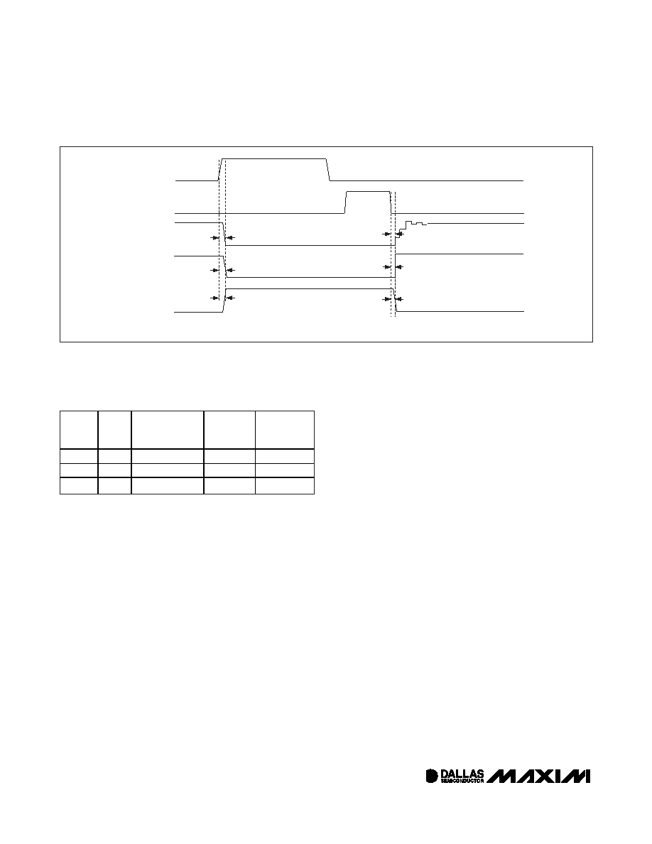
IBIAS
VMOD
DETECTION OF
FETG FAULT
tOFF
tON
tOFF
TX-D
tFETG:ON
FETG*
*FETG DIR = 0
tFETG:OFF
Figure 6. FETG/Modulation and Bias Timing (Fault Condition Detected)
Table 5. FETG, MOD, and BIAS Outputs
as a Function of TX-D and Alarm Sources
VCC >
VPOA
TX-D
NONMASKED
FETG ALARM
FETG
MOD AND
BIAS
OUTPUTS
Yes
0
FETG DIR
Enabled
Yes
0
1
FETG DIR
Disabled
Yes
1
X
FETG DIR
Disabled
相关PDF资料 |
PDF描述 |
|---|---|
| TLE8264E | IC SYSTEM BASIS CHIP DSO-36 |
| MAX4507CWN+T | IC SIGNAL LINE PROTECTOR 18-SOIC |
| TLE8263-2E | IC SYSTEM BASIS CHIP DSO-36 |
| TLE8263E | IC SYSTEM BASIS CHIP DSO-36 |
| TLE8262E | IC SYSTEM BASIS CHIP DSO-36 |
相关代理商/技术参数 |
参数描述 |
|---|---|
| DS1866 | 功能描述:数字电位计 IC RoHS:否 制造商:Maxim Integrated 电阻:200 Ohms 温度系数:35 PPM / C 容差:25 % POT 数量:Dual 每 POT 分接头:256 弧刷存储器:Volatile 缓冲刷: 数字接口:Serial (3-Wire, SPI) 描述/功能:Dual Volatile Low Voltage Linear Taper Digital Potentiometer 工作电源电压:1.7 V to 5.5 V 电源电流:27 uA 最大工作温度:+ 125 C 安装风格:SMD/SMT 封装 / 箱体:TQFN-16 封装:Reel |
| DS1866+ | 功能描述:数字电位计 IC Log Trimmer RoHS:否 制造商:Maxim Integrated 电阻:200 Ohms 温度系数:35 PPM / C 容差:25 % POT 数量:Dual 每 POT 分接头:256 弧刷存储器:Volatile 缓冲刷: 数字接口:Serial (3-Wire, SPI) 描述/功能:Dual Volatile Low Voltage Linear Taper Digital Potentiometer 工作电源电压:1.7 V to 5.5 V 电源电流:27 uA 最大工作温度:+ 125 C 安装风格:SMD/SMT 封装 / 箱体:TQFN-16 封装:Reel |
| DS1866N | 制造商:未知厂家 制造商全称:未知厂家 功能描述:Interface IC |
| DS1866S | 制造商:未知厂家 制造商全称:未知厂家 功能描述:Interface IC |
| DS1866SN | 制造商:未知厂家 制造商全称:未知厂家 功能描述:Interface IC |
发布紧急采购,3分钟左右您将得到回复。