- 您现在的位置:买卖IC网 > Datasheet目录409 > DS1870E-010+T&R (Maxim Integrated)IC CNTRLR RF POWER AMP 16TSSOP Datasheet资料下载
参数资料
| 型号: | DS1870E-010+T&R |
| 厂商: | Maxim Integrated |
| 文件页数: | 12/28页 |
| 文件大小: | 0K |
| 描述: | IC CNTRLR RF POWER AMP 16TSSOP |
| 产品培训模块: | Lead (SnPb) Finish for COTS Obsolescence Mitigation Program |
| 标准包装: | 1,000 |
| RF 型: | 手机 |
| 封装/外壳: | 16-TSSOP(0.173",4.40mm 宽) |
| 供应商设备封装: | 16-TSSOP |
| 包装: | 带卷 (TR) |
第1页第2页第3页第4页第5页第6页第7页第8页第9页第10页第11页当前第12页第13页第14页第15页第16页第17页第18页第19页第20页第21页第22页第23页第24页第25页第26页第27页第28页
�� �
�
�LDMOS� RF� Power-Amplifier� Bias�
�Controller�
�9Ah�
�99h�
�DECREASING�
�TEMPERATURE�
�9Ah�
�99h�
�DECREASING�
�DRAIN� VOLTAGE�
�9Ah�
�99h�
�DECREASING�
�DRAIN� CURRENT�
�98h�
�98h�
�98h�
�97h�
�96h�
�INCREASING�
�TEMPERATURE�
�97h�
�96h�
�INCREASING�
�DRAIN� VOLTAGE�
�97h�
�96h�
�INCREASING�
�DRAIN� CURRENT�
�95h�
�95h�
�95h�
�2�
�4� 6� 8� 10�
�TEMPERATURE� (� °� C)�
�12�
�AA00� AC00� AEOO� B000� B200� B400�
�DRAIN� VOLTAGE� CONVERSION� (HEX)�
�2A00� 2C00� 2E00� 3000� 3200� 3400�
�DRAIN� CURRENT� CONVERSION� (HEX)�
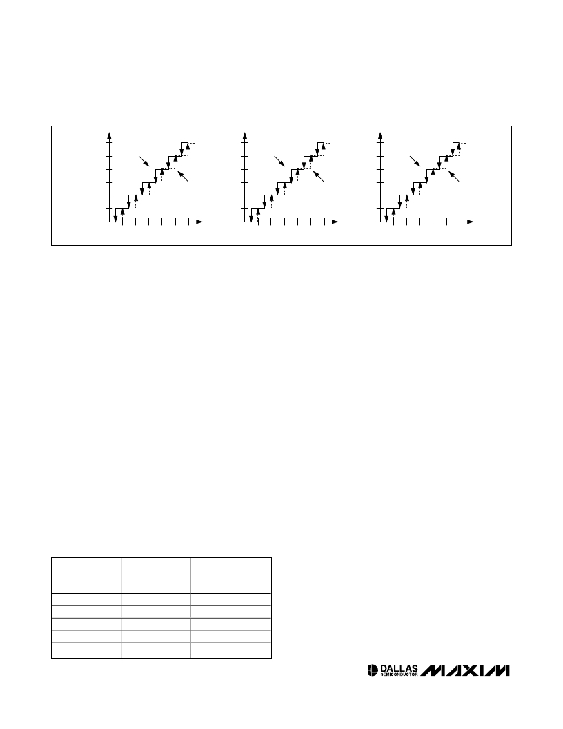
�Figure� 1.� LUT� Hysteresis�
�The� temperature� tables� (LUT� 2� and� LUT� 3)� are� 72� bytes�
�each.� This� allows� the� biasing� to� be� adjusted� every� 2°C�
�between� -40°C� and� +102°C.� Temperatures� less� than�
�-40°C� or� greater� than� +102°C� use� the� -40°C� or� +102°C�
�values,� respectively.� The� values� in� the� temperature�
�tables� are� 8-bit� unsigned� values� (0� to� 255� decimal)� that�
�allow� the� potentiometer� to� be� set� to� any� position� as� a�
�function� of� the� temperature.� The� temperature� LUTs�
�have� 1°C� hysteresis� (Figure� 1)� to� prevent� the� poten-�
�tiometer’s� position� from� chattering� in� the� event� the� tem-�
�perature� remains� near� a� LUT� switching� point.� Table� 5�
�shows� how� the� DS1870� determines� the� temperature�
�tables� index� as� a� function� of� temperature.�
�The� drain� tables� (LUT� 4� and� LUT5)� are� 64� bytes� each,�
�and� they� can� be� indexed� either� by� the� drain� voltage� or�
�the� drain� current� corresponding� to� the� potentiometer.�
�The� VD1� control� bit� determines� if� the� voltage� sensed� on�
�V� D� or� I� D1� adjusts� the� POT1� Drain� LUT,� and� the� VD2�
�control� bit� determines� if� the� voltage� sensed� on� V� D� or�
�I� D2� controls� the� POT2� Drain� LUT.� The� VD1� and� VD2�
�control� bits� are� located� in� register� 85h� of� memory� table�
�1.� The� drain� tables� are� programmed� with� an� 8-bit�
�signed� value� (-128� to� +127� decimal)� that� allow� a� rela-�
�tive� offset� from� the� temperature� LUT� values� determined�
�by� the� amplifier’s� drain� characteristics.�
�Table� 6.� LUT� Addresses� for� V� D� or� I� DX�
�Values�
�The� drain� LUTs� are� indexed� either� by� the� upper� half� of�
�the� V� D� range� or� the� lower� half� of� its� corresponding� I� DX�
�range.� Table� 6� shows� how� the� index� is� determined�
�based� on� the� V� D� or� I� DX� values.� Hysteresis� equal� to�
�0100h� is� also� implemented� on� the� drain� monitor�
�(Figure� 1)� to� ensure� that� voltages� close� to� a� switching�
�point� do� not� cause� the� potentiometer� position� to� chatter�
�between� two� LUT� values.� The� drain� LUT� index� values� are�
�specified� in� hexadecimal� because� the� hexadecimal� val-�
�ues� are� applicable� regardless� of� the� gain� and� offset� cali-�
�bration� of� the� DS1870.�
�Manual� Mode�
�During� normal� operation,� the� potentiometer� position� is�
�automatically� modified� once� per� conversion� cycle�
�based� on� the� ADC� results.� The� DS1870� can� either� stop�
�the� update� function� all� together� by� using� the� B/O_en�
�bit,� or� the� temperature� and� drain� LUT� indexes� can� be�
�manually� controlled� by� using� the� Index_en� bit.� These�
�bits� are� located� in� the� Man� DAC� register� located� in�
�memory� table� 1,� byte� AFh.� More� information� about�
�these� bits� is� in� the� Register� Description� section.�
�Voltage-Monitor� Calibration�
�The� DS1870� can� scale� each� analog� voltage’s� gain� and�
�offset� to� produce� the� desired� digital� result.� Each� of� the�
�inputs� (V� CC� ,� V� D� ,� I� D1� ,� I� D2� )� has� a� unique� register� for� the�
�gain� and� offset� (in� memory� table� 1)� allowing� them� to� be�
�individually� calibrated.� Additionally,� the� DS1870� offers�
�the� ability� to� provide� a� temperature� offset� to� allow� the�
�LUT� ADDRESS�
�(hex)�
�80�
�81�
�82�
�…�
�BE�
�BF�
�V� D� VALUE�
�(hex)�
�≤� 8000�
�8200�
�8400�
�…�
�FC00�
�≥� FE00�
�I� DX� VALUE�
�(hex)�
�0000�
�0200�
�0400�
�…�
�7C00�
�≥� 7E00�
�temperature� measurement� to� be� compensated� to�
�account� for� the� difference� in� temperature� between� the�
�DS1870� and� the� device� it� is� biasing.�
�To� scale� the� gain� and� offset� of� the� converter� for� a� spe-�
�cific� input,� you� must� first� know� the� relationship� between�
�the� analog� input� and� the� expected� digital� result.� The�
�input� that� would� produce� a� digital� result� of� all� zeros� is�
�the� null� value� (normally� this� input� is� GND).� The� input�
�that� would� produce� a� digital� result� of� all� ones� (FFF8h)� is�
�12�
�____________________________________________________________________�
�相关PDF资料 |
PDF描述 |
|---|---|
| DS18S20-PAR+T&R | IC THERM MICROLAN HI-PREC TO-92 |
| DS60R+T&R | IC SENSOR MICRO CENTIGRADE SOT23 |
| DV164102 | KIT DEV RFPICKIT KIT 1 |
| DVK90109 | KIT DEV FOR MLX90109 |
| DVK90121 | KIT DEV FOR MLX90121 |
相关代理商/技术参数 |
参数描述 |
|---|---|
| DS1870K | 制造商:Maxim Integrated Products 功能描述:DS1870 EVALUATION KIT - Bulk |
| DS1873 | 制造商:MAXIM 制造商全称:Maxim Integrated Products 功能描述:SFP+ Controller with Analog LDD Interface |
| DS1873T+ | 功能描述:ADC / DAC多通道 SFP+ Ctrl w/Analog RoHS:否 制造商:Texas Instruments 转换速率: 分辨率:8 bit 接口类型:SPI 电压参考: 电源电压-最大:3.6 V 电源电压-最小:2 V 最大工作温度:+ 85 C 安装风格:SMD/SMT 封装 / 箱体:VQFN-40 |
| DS1873T+T&R | 制造商:Maxim Integrated Products 功能描述:5X5 TQFN SFP+ CTRL W/ANALOG - Tape and Reel 制造商:Maxim Integrated Products 功能描述:IC CTLR SFP+ ANLG LDD 28-TQFN |
| DS1873T+T&R | 功能描述:ADC / DAC多通道 SFP+ Ctrl w/Analog RoHS:否 制造商:Texas Instruments 转换速率: 分辨率:8 bit 接口类型:SPI 电压参考: 电源电压-最大:3.6 V 电源电压-最小:2 V 最大工作温度:+ 85 C 安装风格:SMD/SMT 封装 / 箱体:VQFN-40 |
发布紧急采购,3分钟左右您将得到回复。