- 您现在的位置:买卖IC网 > Datasheet目录409 > DS1870E-010+T&R (Maxim Integrated)IC CNTRLR RF POWER AMP 16TSSOP Datasheet资料下载
参数资料
| 型号: | DS1870E-010+T&R |
| 厂商: | Maxim Integrated |
| 文件页数: | 14/28页 |
| 文件大小: | 0K |
| 描述: | IC CNTRLR RF POWER AMP 16TSSOP |
| 产品培训模块: | Lead (SnPb) Finish for COTS Obsolescence Mitigation Program |
| 标准包装: | 1,000 |
| RF 型: | 手机 |
| 封装/外壳: | 16-TSSOP(0.173",4.40mm 宽) |
| 供应商设备封装: | 16-TSSOP |
| 包装: | 带卷 (TR) |
第1页第2页第3页第4页第5页第6页第7页第8页第9页第10页第11页第12页第13页当前第14页第15页第16页第17页第18页第19页第20页第21页第22页第23页第24页第25页第26页第27页第28页
�� �
�
�LDMOS� RF� Power-Amplifier� Bias�
�Controller�
�As� the� device� powers� up,� the� V� CC� Lo� alarm� flag�
�defaults� to� a� 1� until� the� first� V� CC� ADC� conversion�
�occurs� and� sets� or� clears� the� flag� accordingly.� The�
�FAULT� output� is� active� when� V� CC� <� V� POA� .�
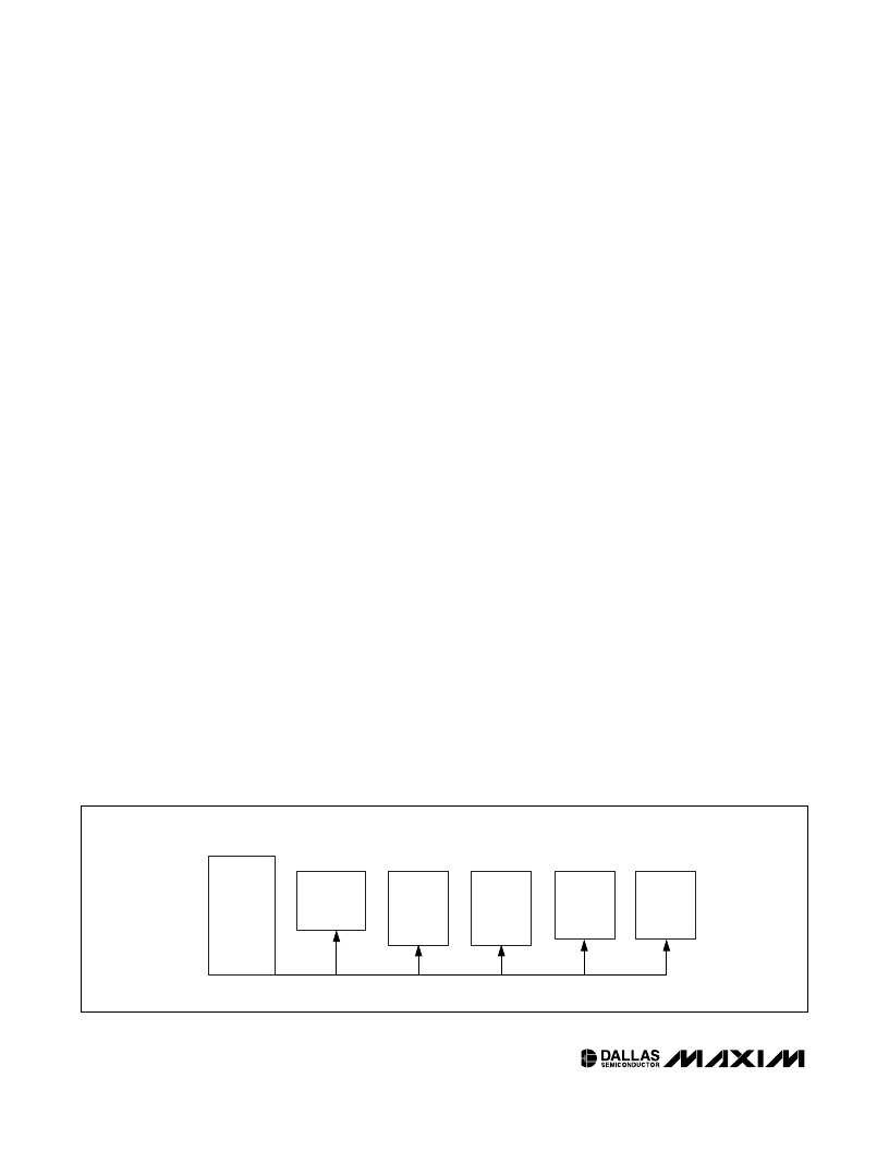
�Memory� Description�
�The� DS1870� memory� map� is� divided� into� six� sections�
�that� include� the� lower� memory� (addresses� 00h� to� 7Fh)�
�and� five� memory� tables� (Figure� 2).� The� memory� tables�
�are� addressed� by� setting� the� table-select� byte� (7Fh)� to�
�the� desired� table� number� and� accessing� the� upper�
�memory� locations� (80h� to� FFh).� The� lower� memory� can�
�be� addressed� at� any� time� regardless� of� the� state� of� the�
�table-select� byte.� The� lower� memory� and� memory� table�
�1� are� used� to� configure� the� DS1870� and� read� the� status�
�of� the� monitors.� The� lower� memory� also� contains� the� 32�
�bytes� of� user� memory.� Memory� tables� 2� and� 3� contain�
�the� base� potentiometer� positions� that� are� used� for� bias-�
�ing� based� on� the� reading� of� the� internal� temperature�
�sensor.� Memory� tables� 4� and� 5� contain� the� relative� off-�
�sets� that� are� added� to� the� base� number� as� a� function� of�
�either� the� drain� voltage� or� the� individual� drain� current�
�monitors.� See� the� Memory� Map� for� a� complete� listing� of�
�registers� and� the� Register� Description� section� for�
�details� about� each� register.�
�Password� Memory� Protection�
�The� DS1870� contains� a� 2-byte� password� that� allows� all�
�of� its� EE� memory� to� be� write� protected� until� the� proper�
�password� is� entered� into� the� password� entry� (PWE)�
�word� (address� 78h).� This� allows� factory� calibration� data�
�for� the� bias� settings,� alarm� thresholds,� and� all� the� other�
�EEPROM� information� to� be� write� protected.� The� pass-�
�word� is� set� by� writing� to� the� Password� register,� which� is�
�the� first� two� bytes� of� memory� table� 1.�
�The� factory� default� value� for� the� password� is� FFFFh,�
�which� is� also� the� factory� default� value� for� PWE� on�
�power-up.� This� means� that� parts� are� unlocked� at�
�power-up� when� they� are� first� received� by� customers.�
�The� password� should� be� programmed� to� a� value� other�
�than� FFFFh� to� ensure� the� calibration� data� is� write� pro-�
�tected.� The� PWE� register� always� reads� 0000h� regard-�
�less� of� its� programmed� value.�
�EEPROM� Write� Disable�
�Memory� locations� 20h� to� 3Fh� and� Table� 1� locations� 80h�
�to� A7h� are� SRAM-shadowed� EEPROM.� By� default�
�(� SEE� =� 0)� these� locations� act� as� ordinary� EEPROM.� By�
�setting� SEE� =� 1,� these� locations� begin� to� function� like�
�SRAM� cells,� which� allow� an� infinite� number� of� write�
�cycles� without� concern� of� wearing� out� the� EEPROM.�
�This� also� eliminates� the� requirement� for� the� EEPROM�
�write� time.� Because� changes� made� with� SEE� =� 1� do� not�
�affect� the� EEPROM,� these� changes� are� not� retained�
�through� power� cycles.� The� power-up� value� is� the� last�
�value� written� with� SEE� =� 0.� This� function� can� be� used� to�
�limit� the� number� of� EEPROM� writes� during� calibration� or�
�to� change� the� monitor� thresholds� periodically� during�
�normal� operation� without� wearing� out� the� EEPROM.� The�
�SEE� bit� resides� in� memory� table� 1,� byte� AFh.�
�Memory� Map�
�The� upper� part� of� the� memory� map� is� organized� into�
�8-byte� or� 4-word� (2-byte)� rows.� The� beginning� address�
�of� the� row� is� shown� in� the� left-most� column� of� the� map,�
�and� is� equal� to� the� byte� 0� or� word� 0� memory� address.�
�The� next� byte� (Byte� 1)� is� located� at� the� next� highest�
�memory� address,� and� the� next� word� (Word� 1)� is� two�
�memory� addresses� greater� than� the� row’s� beginning�
�address.� The� lower� part� of� the� memory� map� expands�
�the� bytes� or� the� words� to� show� the� names� of� the� bits�
�within� the� byte/word,� or� their� bit� weights� (2� X� )� for� regis-�
�ters� that� contain� numerical� information.� Numerical� reg-�
�isters� that� contain� an� “S”� in� the� most� significant� bit� are�
�showing� sign� extension� for� 2’s� complement� numbers.�
�Descriptions� of� each� byte/bit� follow� in� the� Register�
�Description� section.�
�00h�
�MAIN� MEMORY�
�80h�
�TABLE� 1�
�80h�
�TABLE� 2�
�80h�
�TABLE� 3�
�80h�
�TABLE� 4�
�80h�
�TABLE� 5�
�USER� MEMORY;�
�HI/LO� ALARM�
�THRESHOLDS;�
�ADC� RESULTS;� AFh�
�CONFIGURATION�
�CONFIGURATION�
�SEL�
�C7h�
�POT1�
�TEMP�
�LUT�
�SEL�
�C7h�
�POT2�
�TEMP�
�LUT�
�SEL�
�BFh�
�POT1�
�DRAIN�
�LUT�
�SEL�
�BFh�
�POT2�
�DRAIN�
�LUT�
�SEL�
�TABLE-SELECT�
�7Fh�
�Figure� 2.� Memory� Organization�
�BYTE� (7Fh)�
�14�
�____________________________________________________________________�
�相关PDF资料 |
PDF描述 |
|---|---|
| DS18S20-PAR+T&R | IC THERM MICROLAN HI-PREC TO-92 |
| DS60R+T&R | IC SENSOR MICRO CENTIGRADE SOT23 |
| DV164102 | KIT DEV RFPICKIT KIT 1 |
| DVK90109 | KIT DEV FOR MLX90109 |
| DVK90121 | KIT DEV FOR MLX90121 |
相关代理商/技术参数 |
参数描述 |
|---|---|
| DS1870K | 制造商:Maxim Integrated Products 功能描述:DS1870 EVALUATION KIT - Bulk |
| DS1873 | 制造商:MAXIM 制造商全称:Maxim Integrated Products 功能描述:SFP+ Controller with Analog LDD Interface |
| DS1873T+ | 功能描述:ADC / DAC多通道 SFP+ Ctrl w/Analog RoHS:否 制造商:Texas Instruments 转换速率: 分辨率:8 bit 接口类型:SPI 电压参考: 电源电压-最大:3.6 V 电源电压-最小:2 V 最大工作温度:+ 85 C 安装风格:SMD/SMT 封装 / 箱体:VQFN-40 |
| DS1873T+T&R | 制造商:Maxim Integrated Products 功能描述:5X5 TQFN SFP+ CTRL W/ANALOG - Tape and Reel 制造商:Maxim Integrated Products 功能描述:IC CTLR SFP+ ANLG LDD 28-TQFN |
| DS1873T+T&R | 功能描述:ADC / DAC多通道 SFP+ Ctrl w/Analog RoHS:否 制造商:Texas Instruments 转换速率: 分辨率:8 bit 接口类型:SPI 电压参考: 电源电压-最大:3.6 V 电源电压-最小:2 V 最大工作温度:+ 85 C 安装风格:SMD/SMT 封装 / 箱体:VQFN-40 |
发布紧急采购,3分钟左右您将得到回复。