- 您现在的位置:买卖IC网 > PDF目录11783 > DS1875T+ (Maxim Integrated Products)IC SFP CTRLR/TRIPLEXER 38-TQFN PDF资料下载
参数资料
| 型号: | DS1875T+ |
| 厂商: | Maxim Integrated Products |
| 文件页数: | 63/92页 |
| 文件大小: | 0K |
| 描述: | IC SFP CTRLR/TRIPLEXER 38-TQFN |
| 产品培训模块: | Lead (SnPb) Finish for COTS Obsolescence Mitigation Program |
| 标准包装: | 90 |
| 应用: | 光纤 |
| 接口: | I²C |
| 电源电压: | 2.85 V ~ 3.9 V |
| 封装/外壳: | 38-WFQFN 裸露焊盘 |
| 供应商设备封装: | 38-TQFN(5x7) |
| 包装: | 管件 |
| 安装类型: | 表面贴装 |
| 产品目录页面: | 1431 (CN2011-ZH PDF) |
第1页第2页第3页第4页第5页第6页第7页第8页第9页第10页第11页第12页第13页第14页第15页第16页第17页第18页第19页第20页第21页第22页第23页第24页第25页第26页第27页第28页第29页第30页第31页第32页第33页第34页第35页第36页第37页第38页第39页第40页第41页第42页第43页第44页第45页第46页第47页第48页第49页第50页第51页第52页第53页第54页第55页第56页第57页第58页第59页第60页第61页第62页当前第63页第64页第65页第66页第67页第68页第69页第70页第71页第72页第73页第74页第75页第76页第77页第78页第79页第80页第81页第82页第83页第84页第85页第86页第87页第88页第89页第90页第91页第92页
DS1875
PON Triplexer and SFP Controller
66
______________________________________________________________________________________
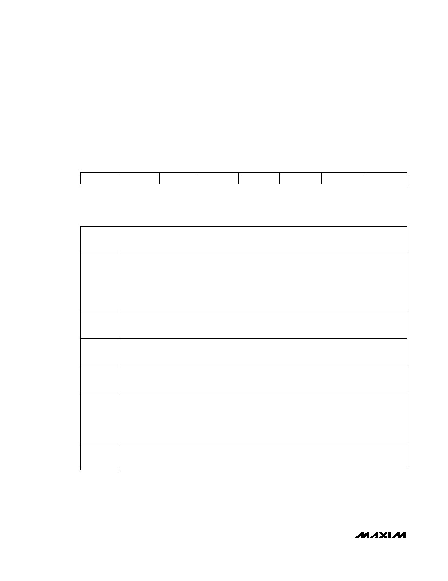
Table 02h, Register 89h: CONFIG
FACTORY DEFAULT
00h
READ ACCESS
PW2
WRITE ACCESS
PW2
MEMORY TYPE
Nonvolatile (SEE)
89h
FETG DIR
TX-F LEN
M3QT LEN
ASEL
BOLFS
RSSI_FC
RSSI_FF
EN5TO8B
BIT 7
BIT 0
Configure the memory location and the polarity of the digital outputs.
BIT 7
FETG DIR: Chooses the direction or polarity of the FETG output for normal operation.
0 = (Default) Under normal operation, FETG is pulled low.
1 = Under normal operation, FETG is pulled high.
BIT 6
TX-F LEN: The TX-F output pin always reflects the wired-OR of all TX-F enabled alarm states. This
bit enables the latching of the alarm state for the TX-F output pin.
0 = (Default) Not latched.
1 = The alarm bits are latched until cleared by a TX-D transition or power-down. If the VCC alarm is
enabled for either FETG or TX-F, then latching is disabled until after the first VCC measurement is
made above the VCC ALARM LO set point to allow for proper operation during slow power-on
cycles.
BIT 5
M3QT LEN: This bit enables the latching of the alarm for the M3QT.
0 = (Default) Not latched.
1 = The alarm bit is latched until cleared by setting the M3QT RESET bit (Byte 78h).
BIT 4
ASEL: Address select.
0 = (Default) Device address of A2h.
1 = Device address is equal to the value found in the DEVICE ADDRESS byte (Table 02h, 8Ch).
BIT 3
BOLFS: Bias open-loop full scale.
0 = (Default) Full scale is 600μA.
1 = Full scale is 1.2mA.
BITS 2:1
RSSI_FC and RSSI_FF: RSSI force coarse and RSSI force fine. Control bits for RSSI mode of
operation on the MON3 conversion.
00b = (Default) Normal RSSI mode of operation.
01b = The fine settings of scale and offset are used for MON3 conversions.
10b = The coarse settings of scale and offset are used for MON3 conversions.
11b = Normal RSSI mode of operation.
BIT 0
EN5TO8B: This bit enables MON5–MON8 conversion (voltage of D0–D3 pins).
0 = (Default) Temperature, VCC, and MON1–MON8 conversions are enabled.
1 = Temperature, VCC, and MON1–MON4 conversions are enabled.
相关PDF资料 |
PDF描述 |
|---|---|
| D38999/20MD18PA | CONN RCPT 18POS WALL MNT W/PINS |
| MAX7359ETG+ | IC KEY SWITCH 2WIRE 24-TQFN |
| USB-232-SS | IC USB ASYNC SRL UART 20-SSOP |
| MS27473E24F61P | CONN PLUG 61POS STRAIGHT W/PINS |
| MS27474E10F98PA | CONN RCPT 6POS JAM NUT W/PINS |
相关代理商/技术参数 |
参数描述 |
|---|---|
| DS1875T+ | 功能描述:ADC / DAC多通道 PON Triplexer & SFP Controller RoHS:否 制造商:Texas Instruments 转换速率: 分辨率:8 bit 接口类型:SPI 电压参考: 电源电压-最大:3.6 V 电源电压-最小:2 V 最大工作温度:+ 85 C 安装风格:SMD/SMT 封装 / 箱体:VQFN-40 |
| DS1875T+T&R | 制造商:Maxim Integrated Products 功能描述:PON TRIPLEXER 38TQFN EP - Tape and Reel 制造商:Maxim Integrated Products 功能描述:IC SFP CTRLR/TRIPLEXER 38-TQFN 制造商:Maxim Integrated Products 功能描述:ADC / DAC Multichannel PON Triplexer & SFP Controller |
| DS1875T+T&R | 功能描述:ADC / DAC多通道 PON Triplexer & SFP Controller RoHS:否 制造商:Texas Instruments 转换速率: 分辨率:8 bit 接口类型:SPI 电压参考: 电源电压-最大:3.6 V 电源电压-最小:2 V 最大工作温度:+ 85 C 安装风格:SMD/SMT 封装 / 箱体:VQFN-40 |
| DS1875T+TR | 制造商:MAXIM 制造商全称:Maxim Integrated Products 功能描述:PON Triplexer and SFP Controller |
| DS1876 | 制造商:MAXIM 制造商全称:Maxim Integrated Products 功能描述:SFP Controller with Dual LDD Interface |
发布紧急采购,3分钟左右您将得到回复。