- 您现在的位置:买卖IC网 > Datasheet目录322 > DS2045W-100# (Maxim Integrated)IC NVSRAM 1MBIT 100NS 256BGA Datasheet资料下载
参数资料
| 型号: | DS2045W-100# |
| 厂商: | Maxim Integrated |
| 文件页数: | 6/12页 |
| 文件大小: | 0K |
| 描述: | IC NVSRAM 1MBIT 100NS 256BGA |
| 标准包装: | 1 |
| 格式 - 存储器: | RAM |
| 存储器类型: | NVSRAM(非易失 SRAM) |
| 存储容量: | 1M (128K x 8) |
| 速度: | 100ns |
| 接口: | 并联 |
| 电源电压: | 3 V ~ 3.6 V |
| 工作温度: | -40°C ~ 85°C |
| 封装/外壳: | 256-BBGA |
| 供应商设备封装: | 256-BGA(27x27) |
| 包装: | 托盘 |
�� �
�
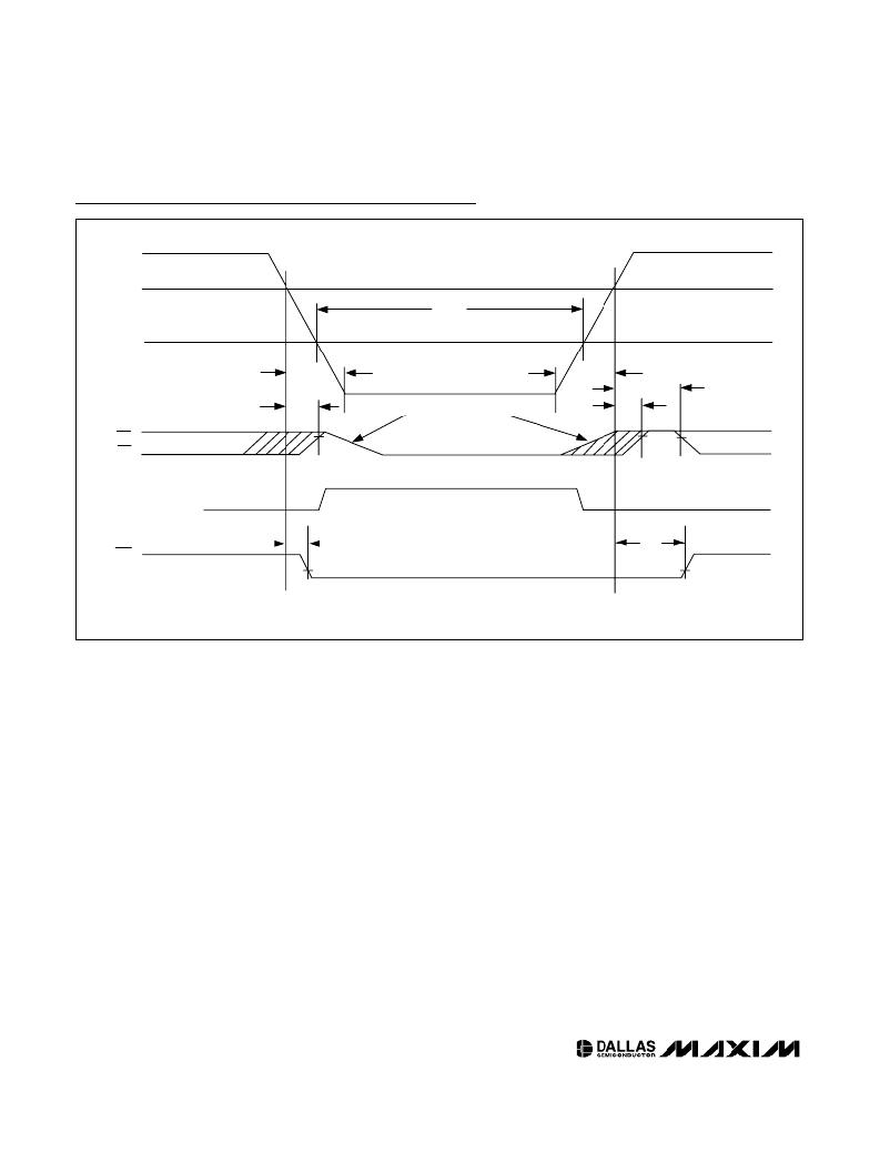
�DS2045W� 3.3V� Single-Piece� 1Mb�
�Nonvolatile� SRAM�
�Power-Down/Power-Up� Condition�
�V� CC�
�V� TP�
�t� DR�
�~� 2.5V�
�t� F�
�t� R�
�t� REC�
�CE,�
�WE�
�BACKUP� CURRENT�
�SUPPLIED� FROM�
�LITHIUM� BATTERY�
�RST�
�t� PD�
�V� OL�
�t� RPD�
�SLEWS� WITH�
�V� CC�
�t� PU�
�t� RPU�
�V� OL�
�V� IH�
�(SEE� NOTES� 1,� 7.)�
�Note� 1:� RST� is� an� open-drain� output� and� cannot� source� current.� An� external� pullup� resistor� should� be� connected� to� this� pin� to� real-�
�ize� a� logic-high� level.�
�Note� 2:� These� parameters� are� sampled� with� a� 5pF� load� and� are� not� 100%� tested.�
�Note� 3:� t� WP� is� specified� as� the� logical� AND� of� CE� and� WE� .� t� WP� is� measured� from� the� latter� of� CE� or� WE� going� low� to� the� earlier� of�
�CE� or� WE� going� high.�
�Note� 4:� t� WR1� and� t� DH1� are� measured� from� WE� going� high.�
�Note� 5:� t� WR2� and� t� DH2� are� measured� from� CE� going� high.�
�Note� 6:� t� DS� is� measured� from� the� earlier� of� CE� or� WE� going� high.�
�Note� 7:� In� a� power-down� condition,� the� voltage� on� any� pin� can� not� exceed� the� voltage� on� V� CC� .�
�Note� 8:� The� expected� t� DR� is� defined� as� accumulative� time� in� the� absence� of� V� CC� starting� from� the� time� power� is� first� applied� by� the�
�user.� Minimum� expected� data-retention� time� is� based� on� a� maximum� of� two� +230°C� convection� solder� reflow� exposures,�
�followed� by� a� fully� charged� cell.� Full� charge� occurs� with� the� initial� application� of� V� CC� for� a� minimum� of� 96� hours.� This� para-�
�meter� is� assured� by� component� selection,� process� control,� and� design.� It� is� not� measured� directly� in� production� testing.�
�Note� 9:� WE� is� high� for� a� read� cycle.�
�Note� 10:� OE� =� V� IH� or� V� IL� .� If� OE� =� V� IH� during� write� cycle,� the� output� buffers� remain� in� a� high-impedance� state.�
�Note� 11:� If� the� CE� low� transition� occurs� simultaneously� with� or� latter� than� the� WE� low� transition,� the� output� buffers� remain� in� a� high-�
�impedance� state� during� this� period.�
�Note� 12:� If� the� CE� high� transition� occurs� prior� to� or� simultaneously� with� the� WE� high� transition,� the� output� buffers� remain� in� a� high-�
�impedance� state� during� this� period.�
�Note� 13:� If� WE� is� low� or� the� WE� low� transition� occurs� prior� to� or� simultaneously� with� the� CE� low� transition,� the� output� buffers� remain�
�in� a� high-impedance� state� during� this� period.�
�Note� 14:� DS2045W� BGA� modules� are� recognized� by� Underwriters� Laboratory� (UL)� under� file� E99151.�
�6�
�_____________________________________________________________________�
�相关PDF资料 |
PDF描述 |
|---|---|
| DS2045Y-70# | IC NVSRAM 1MBIT 70NS 256BGA |
| DS2050W-100# | IC NVSRAM 4MBIT 100NS 256BGA |
| DS2065W-100# | IC NVSRAM 8MBIT 100NS 256BGA |
| DS2070W-100# | IC NVSRAM 16MBIT 100NS 256BGA |
| DS2227-070 | IC NVSRAM 4MBIT 70NS 72SIMM |
相关代理商/技术参数 |
参数描述 |
|---|---|
| DS2045W-100# | 功能描述:NVRAM RoHS:否 制造商:Maxim Integrated 数据总线宽度:8 bit 存储容量:1024 Kbit 组织:128 K x 8 接口类型:Parallel 访问时间:70 ns 电源电压-最大:5.5 V 电源电压-最小:4.5 V 工作电流:85 mA 最大工作温度:+ 70 C 最小工作温度:0 C 封装 / 箱体:EDIP 封装:Tube |
| DS2045Y | 制造商:DALLAS 制造商全称:Dallas Semiconductor 功能描述:Single-Piece 1Mb Nonvolatile SRAM |
| DS2045Y-100 | 功能描述:NVRAM RoHS:否 制造商:Maxim Integrated 数据总线宽度:8 bit 存储容量:1024 Kbit 组织:128 K x 8 接口类型:Parallel 访问时间:70 ns 电源电压-最大:5.5 V 电源电压-最小:4.5 V 工作电流:85 mA 最大工作温度:+ 70 C 最小工作温度:0 C 封装 / 箱体:EDIP 封装:Tube |
| DS2045Y-100# | 功能描述:NVRAM RoHS:否 制造商:Maxim Integrated 数据总线宽度:8 bit 存储容量:1024 Kbit 组织:128 K x 8 接口类型:Parallel 访问时间:70 ns 电源电压-最大:5.5 V 电源电压-最小:4.5 V 工作电流:85 mA 最大工作温度:+ 70 C 最小工作温度:0 C 封装 / 箱体:EDIP 封装:Tube |
| DS2045Y20# | 制造商:Maxim Integrated Products 功能描述: |
发布紧急采购,3分钟左右您将得到回复。