参数资料
| 型号: | DS3994Z+T&R |
| 厂商: | Maxim Integrated |
| 文件页数: | 24/28页 |
| 文件大小: | 0K |
| 描述: | IC CCFL CNTRLR 4CH 28-SOIC |
| 产品培训模块: | Lead (SnPb) Finish for COTS Obsolescence Mitigation Program |
| 标准包装: | 1,000 |
| 类型: | CCFL 控制器 |
| 频率: | 20 ~ 80 kHz |
| 电流 - 电源: | 9mA |
| 电源电压: | 4.5 V ~ 5.5 V |
| 工作温度: | -40°C ~ 85°C |
| 封装/外壳: | 28-SOIC(0.295",7.50mm 宽) |
| 供应商设备封装: | 28-SOIC W |
| 包装: | 带卷 (TR) |
第1页第2页第3页第4页第5页第6页第7页第8页第9页第10页第11页第12页第13页第14页第15页第16页第17页第18页第19页第20页第21页第22页第23页当前第24页第25页第26页第27页第28页
�� �
�
�4-Channel� Cold-Cathode�
�Fluorescent� Lamp� Controller�
�Byte� Write:� A� byte� write� consists� of� 8� bits� of� informa-�
�tion� transferred� from� the� master� to� the� slave� (most� sig-�
�nificant� bit� first)� plus� a� 1-bit� acknowledgement� from� the�
�slave� to� the� master.� The� 8� bits� transmitted� by� the� mas-�
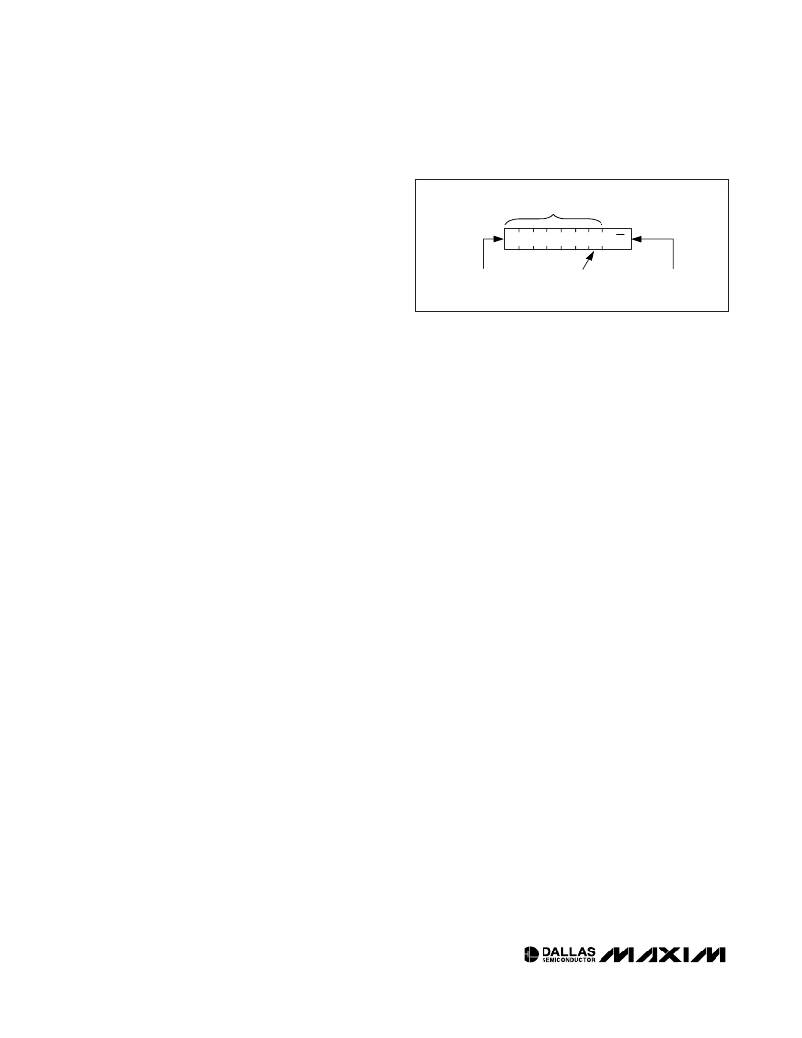
�7-BIT� SLAVE� ADDRESS�
�ter� are� done� according� to� the� bit-write� definition� and� the�
�1�
�0�
�1�
�0�
�0�
�0� A� 0�
�R/W�
�acknowledgement� is� read� using� the� bit-read� definition.�
�Byte� Read:� A� byte� read� is� an� 8-bit� information� transfer�
�from� the� slave� to� the� master� plus� a� 1-bit� ACK� or� NACK�
�MOST�
�SIGNIFICANT� BIT�
�A� 0� PIN� VALUE�
�DETERMINES�
�READ� OR� WRITE�
�from� the� master� to� the� slave.� The� 8� bits� of� information�
�that� are� transferred� (most� significant� bit� first)� from� the�
�slave� to� the� master� are� read� by� the� master� using� the� bit�
�read� definition,� and� the� master� transmits� an� ACK� using�
�the� bit� write� definition� to� receive� additional� data� bytes.�
�The� master� must� NACK� the� last� byte� read� to� terminate�
�communication� so� the� slave� will� return� control� of� SDA� to�
�the� master.�
�Slave� Address� Byte:� Each� slave� on� the� I� 2� C� bus�
�responds� to� a� slave� addressing� byte� sent� immediately�
�following� a� start� condition.� The� slave� address� byte�
�(Figure� 11)� contains� the� slave� address� in� the� most� signifi-�
�cant� seven� bits� and� the� R/� W� bit� in� the� least� significant� bit.�
�The� DS3994� ’s� slave� address� is� 101000A� 0� (binary),�
�where� A� 0� is� the� value� of� the� address� pin� (A� 0� ).� The�
�address� pin� allows� the� device� to� respond� to� one� of� two�
�possible� slave� addresses.� By� writing� the� correct� slave�
�address� with� R/� W� =� 0,� the� master� writes� data� to� the�
�slave.� If� R/� W� =� 1,� the� master� reads� data� from� the� slave.�
�If� an� incorrect� slave� address� is� written,� the� DS3994� will�
�assume� the� master� is� communicating� with� another� I� 2� C�
�device� and� ignore� the� communications� until� the� next�
�start� condition� is� sent.�
�Memory� Address:� During� an� I� 2� C� write� operation,� the�
�master� must� transmit� a� memory� address� to� identify� the�
�memory� location� where� the� slave� is� to� store� the� data.�
�The� memory� address� is� always� the� second� byte� trans-�
�mitted� during� a� write� operation� following� the� slave�
�address� byte.�
�Figure� 11.� DS3994’s� Slave� Address� Byte�
�I� 2� C� Communication�
�Writing� a� Data� Byte� to� a� Slave:� The� master� must� gen-�
�erate� a� start� condition,� write� the� slave� address� byte�
�(R/� W� =� 0),� write� the� memory� address,� write� the� byte� of�
�data,� and� generate� a� stop� condition.� Remember� the�
�master� must� read� the� slave’s� acknowledgement� during�
�all� byte� write� operations.� See� Figure� 12� for� more� detail.�
�Acknowledge� Polling:� Any� time� EEPROM� is� written,�
�the� DS3994� requires� the� EEPROM� write� time� (t� W� )� after�
�the� stop� condition� to� write� the� contents� to� EEPROM.�
�During� the� EEPROM� write� time,� the� DS3994� will� not�
�acknowledge� its� slave� address� because� it� is� busy.� It� is�
�possible� to� take� advantage� of� that� phenomenon� by�
�repeatedly� addressing� the� DS3994,� which� allows� the�
�next� byte� of� data� to� be� written� as� soon� as� the� DS3994� is�
�ready� to� receive� the� data.� The� alternative� to� acknowl-�
�edge� polling� is� to� wait� for� a� maximum� period� of� t� W� to�
�elapse� before� attempting� to� write� again� to� the� DS3994.�
�EEPROM� Write� Cycles:� The� number� of� times� the�
�DS3994� ’s� EEPROM� can� be� written� before� it� fails� is�
�specified� in� the� Nonvolatile� Memory� Characteristics�
�table.� This� specification� is� shown� at� the� worst-case�
�write� temperature.� The� DS3994� is� typically� capable� of�
�handling� many� additional� write� cycles� when� the� writes�
�are� performed� at� room� temperature.�
�Reading� a� Data� Byte� from� a� Slave:� To� read� a� single�
�byte� from� the� slave� the� master� generates� a� start� condi-�
�tion,� writes� the� slave� address� byte� with� R/� W� =� 0,� writes�
�the� memory� address,� generates� a� repeated� start� condi-�
�tion,� writes� the� slave� address� with� R/� W� =� 1,� reads� the�
�data� byte� with� a� NACK� to� indicate� the� end� of� the� trans-�
�fer,� and� generates� a� stop� condition.� See� Figure� 12� for�
�more� detail.�
�24�
�____________________________________________________________________�
�相关PDF资料 |
PDF描述 |
|---|---|
| DS4303R-U+ | IC VREF SERIES ADJ SOT-23-5 |
| DS4510U-5/T&R | IC SUPERVISOR W/NV MEM 5-USOP |
| DS4510U+ | IC SUPERVISOR W/NV MEM 10-USOP |
| DW-16-12-G-D-665 | CONN HEADER 32POS DUAL 2.54MM AU |
| DW-22-12-G-T-670 | CONN HEADER 66POS TRIPLE 2.54MM |
相关代理商/技术参数 |
参数描述 |
|---|---|
| DS3CC | 制造商:Thomas & Betts 功能描述:30A,MG,CUP CAP |
| DS3DS3801 | 制造商:Rochester Electronics LLC 功能描述: 制造商:Maxim Integrated Products 功能描述: |
| DS3-LD-015 | 制造商:IDEC CORPORATION 功能描述:957600120 Sensor light grids |
| DS3-LD-030 | 制造商:IDEC CORPORATION 功能描述:957600140 Light grids |
| DS3-LD-045 | 制造商:IDEC CORPORATION 功能描述:957600160 Light grids |
发布紧急采购,3分钟左右您将得到回复。