- 您现在的位置:买卖IC网 > PDF目录11481 > DSPIC33FJ12MC202T-I/SS (Microchip Technology)IC DSPIC MCU/DSP 12K 28SSOP PDF资料下载
参数资料
| 型号: | DSPIC33FJ12MC202T-I/SS |
| 厂商: | Microchip Technology |
| 文件页数: | 68/155页 |
| 文件大小: | 0K |
| 描述: | IC DSPIC MCU/DSP 12K 28SSOP |
| 产品培训模块: | Asynchronous Stimulus |
| 标准包装: | 2,100 |
| 系列: | dsPIC™ 33F |
| 核心处理器: | dsPIC |
| 芯体尺寸: | 16-位 |
| 速度: | 40 MIP |
| 连通性: | I²C,IrDA,SPI,UART/USART |
| 外围设备: | 高级欠压探测/复位,电机控制 PWM,QEI,POR,PWM,WDT |
| 输入/输出数: | 21 |
| 程序存储器容量: | 12KB(12K x 8) |
| 程序存储器类型: | 闪存 |
| RAM 容量: | 1K x 8 |
| 电压 - 电源 (Vcc/Vdd): | 3 V ~ 3.6 V |
| 数据转换器: | A/D 6x10b/12b |
| 振荡器型: | 内部 |
| 工作温度: | -40°C ~ 85°C |
| 封装/外壳: | 28-SSOP(0.209",5.30mm 宽) |
| 包装: | 带卷 (TR) |
第1页第2页第3页第4页第5页第6页第7页第8页第9页第10页第11页第12页第13页第14页第15页第16页第17页第18页第19页第20页第21页第22页第23页第24页第25页第26页第27页第28页第29页第30页第31页第32页第33页第34页第35页第36页第37页第38页第39页第40页第41页第42页第43页第44页第45页第46页第47页第48页第49页第50页第51页第52页第53页第54页第55页第56页第57页第58页第59页第60页第61页第62页第63页第64页第65页第66页第67页当前第68页第69页第70页第71页第72页第73页第74页第75页第76页第77页第78页第79页第80页第81页第82页第83页第84页第85页第86页第87页第88页第89页第90页第91页第92页第93页第94页第95页第96页第97页第98页第99页第100页第101页第102页第103页第104页第105页第106页第107页第108页第109页第110页第111页第112页第113页第114页第115页第116页第117页第118页第119页第120页第121页第122页第123页第124页第125页第126页第127页第128页第129页第130页第131页第132页第133页第134页第135页第136页第137页第138页第139页第140页第141页第142页第143页第144页第145页第146页第147页第148页第149页第150页第151页第152页第153页第154页第155页
PIC18F2XK20/4XK20
DS41303G-page 294
2010 Microchip Technology Inc.
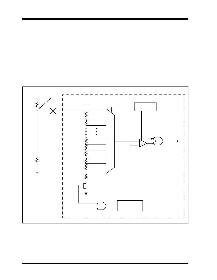
22.1
Operation
When the HLVD module is enabled, a comparator uses
an internally generated reference voltage as the set
point. The set point is compared with the trip point,
where each node in the resistor divider represents a
trip point voltage. The “trip point” voltage is the voltage
level at which the device detects a high or low-voltage
event, depending on the configuration of the module.
When the supply voltage is equal to the trip point, the
voltage tapped off of the resistor array is equal to the
internal reference voltage generated by the voltage
reference module. The comparator then generates an
interrupt signal by setting the HLVDIF bit.
The trip point voltage is software programmable to any
one of 16 values. The trip point is selected by
programming the HLVDL<3:0> bits of the HLVDCON
register.
The HLVD module has an additional feature that allows
the user to supply the trip voltage to the module from
an external source. This mode is enabled when bits
HLVDL<3:0> are set to ‘1111’. In this state, the
comparator input is multiplexed from the external input
pin, HLVDIN. This gives users flexibility because it
allows them to configure the High/Low-Voltage Detect
interrupt to occur at any voltage in the valid operating
range.
FIGURE 22-1:
HLVD MODULE BLOCK DIAGRAM (WITH EXTERNAL INPUT)
Set
VDD
16-to
-1
MUX
HLVDEN
HLVDCON
HLVDIN
HLVDL<3:0>
Register
HLVDIN
VDD
Externally Generated
Trip Point
HLVDIF
HLVDEN
BOREN
Internal Voltage
Reference
VDIRMAG
相关PDF资料 |
PDF描述 |
|---|---|
| PIC18F67J10T-I/PT | IC PIC MCU FLASH 64KX16 64TQFP |
| ADG509FBRNZ | IC MULTIPLEXER DUAL 4X1 16SOIC |
| PIC16C770T-I/SS | IC MCU OTP 2KX14 A/D PWM 20SSOP |
| PIC16LC711-04E/P | IC MCU OTP 1KX14 A/D 18DIP |
| VE-BNF-CU-F2 | CONVERTER MOD DC/DC 72V 200W |
相关代理商/技术参数 |
参数描述 |
|---|---|
| dsPIC33FJ16GP101-E/P | 功能描述:数字信号处理器和控制器 - DSP, DSC 16bit DSC Fam 16MIPS 16KB FL 1KB RAM RoHS:否 制造商:Microchip Technology 核心:dsPIC 数据总线宽度:16 bit 程序存储器大小:16 KB 数据 RAM 大小:2 KB 最大时钟频率:40 MHz 可编程输入/输出端数量:35 定时器数量:3 设备每秒兆指令数:50 MIPs 工作电源电压:3.3 V 最大工作温度:+ 85 C 封装 / 箱体:TQFP-44 安装风格:SMD/SMT |
| dsPIC33FJ16GP101-E/SO | 功能描述:数字信号处理器和控制器 - DSP, DSC 16bit DSC Fam 16MIPS 16KB FL 1KB RAM RoHS:否 制造商:Microchip Technology 核心:dsPIC 数据总线宽度:16 bit 程序存储器大小:16 KB 数据 RAM 大小:2 KB 最大时钟频率:40 MHz 可编程输入/输出端数量:35 定时器数量:3 设备每秒兆指令数:50 MIPs 工作电源电压:3.3 V 最大工作温度:+ 85 C 封装 / 箱体:TQFP-44 安装风格:SMD/SMT |
| dsPIC33FJ16GP101-E/SS | 功能描述:数字信号处理器和控制器 - DSP, DSC 16bit DSC Fam 16MIPS 16KB FL 1KB RAM RoHS:否 制造商:Microchip Technology 核心:dsPIC 数据总线宽度:16 bit 程序存储器大小:16 KB 数据 RAM 大小:2 KB 最大时钟频率:40 MHz 可编程输入/输出端数量:35 定时器数量:3 设备每秒兆指令数:50 MIPs 工作电源电压:3.3 V 最大工作温度:+ 85 C 封装 / 箱体:TQFP-44 安装风格:SMD/SMT |
| dsPIC33FJ16GP101-I/P | 功能描述:数字信号处理器和控制器 - DSP, DSC 16bit DSC Fam 16MIPS 16KB FL 1KB RAM RoHS:否 制造商:Microchip Technology 核心:dsPIC 数据总线宽度:16 bit 程序存储器大小:16 KB 数据 RAM 大小:2 KB 最大时钟频率:40 MHz 可编程输入/输出端数量:35 定时器数量:3 设备每秒兆指令数:50 MIPs 工作电源电压:3.3 V 最大工作温度:+ 85 C 封装 / 箱体:TQFP-44 安装风格:SMD/SMT |
| dsPIC33FJ16GP101-I/SO | 功能描述:数字信号处理器和控制器 - DSP, DSC 16bit DSC Fam 16MIPS 16KB FL 1KB RAM RoHS:否 制造商:Microchip Technology 核心:dsPIC 数据总线宽度:16 bit 程序存储器大小:16 KB 数据 RAM 大小:2 KB 最大时钟频率:40 MHz 可编程输入/输出端数量:35 定时器数量:3 设备每秒兆指令数:50 MIPs 工作电源电压:3.3 V 最大工作温度:+ 85 C 封装 / 箱体:TQFP-44 安装风格:SMD/SMT |
发布紧急采购,3分钟左右您将得到回复。