- 您现在的位置:买卖IC网 > PDF目录11481 > DSPIC33FJ12MC202T-I/SS (Microchip Technology)IC DSPIC MCU/DSP 12K 28SSOP PDF资料下载
参数资料
| 型号: | DSPIC33FJ12MC202T-I/SS |
| 厂商: | Microchip Technology |
| 文件页数: | 81/155页 |
| 文件大小: | 0K |
| 描述: | IC DSPIC MCU/DSP 12K 28SSOP |
| 产品培训模块: | Asynchronous Stimulus |
| 标准包装: | 2,100 |
| 系列: | dsPIC™ 33F |
| 核心处理器: | dsPIC |
| 芯体尺寸: | 16-位 |
| 速度: | 40 MIP |
| 连通性: | I²C,IrDA,SPI,UART/USART |
| 外围设备: | 高级欠压探测/复位,电机控制 PWM,QEI,POR,PWM,WDT |
| 输入/输出数: | 21 |
| 程序存储器容量: | 12KB(12K x 8) |
| 程序存储器类型: | 闪存 |
| RAM 容量: | 1K x 8 |
| 电压 - 电源 (Vcc/Vdd): | 3 V ~ 3.6 V |
| 数据转换器: | A/D 6x10b/12b |
| 振荡器型: | 内部 |
| 工作温度: | -40°C ~ 85°C |
| 封装/外壳: | 28-SSOP(0.209",5.30mm 宽) |
| 包装: | 带卷 (TR) |
第1页第2页第3页第4页第5页第6页第7页第8页第9页第10页第11页第12页第13页第14页第15页第16页第17页第18页第19页第20页第21页第22页第23页第24页第25页第26页第27页第28页第29页第30页第31页第32页第33页第34页第35页第36页第37页第38页第39页第40页第41页第42页第43页第44页第45页第46页第47页第48页第49页第50页第51页第52页第53页第54页第55页第56页第57页第58页第59页第60页第61页第62页第63页第64页第65页第66页第67页第68页第69页第70页第71页第72页第73页第74页第75页第76页第77页第78页第79页第80页当前第81页第82页第83页第84页第85页第86页第87页第88页第89页第90页第91页第92页第93页第94页第95页第96页第97页第98页第99页第100页第101页第102页第103页第104页第105页第106页第107页第108页第109页第110页第111页第112页第113页第114页第115页第116页第117页第118页第119页第120页第121页第122页第123页第124页第125页第126页第127页第128页第129页第130页第131页第132页第133页第134页第135页第136页第137页第138页第139页第140页第141页第142页第143页第144页第145页第146页第147页第148页第149页第150页第151页第152页第153页第154页第155页
2007-2011 Microchip Technology Inc.
DS70265E-page 31
dsPIC33FJ12MC201/202
4.0
MEMORY ORGANIZATION
The dsPIC33FJ12MC201/202 architecture features
separate program and data memory spaces and
buses. This architecture also allows the direct access
of program memory from the data space during code
execution.
4.1
Program Address Space
The program address memory space of the
dsPIC33FJ12MC201/202 devices is 4M instructions.
The space is addressable by a 24-bit value derived
either from the 23-bit Program Counter (PC) during
program execution, or from table operation or data
space remapping as described in Section 4.6
.
User application access to the program memory space
is restricted to the lower half of the address range
(0x000000 to 0x7FFFFF). The exception is the use of
TBLRD/TBLWT
operations, which use TBLPAG<7> to
permit access to the Configuration bits and Device ID
sections of the configuration memory space.
The memory map for the dsPIC33FJ12MC201/202
family of devices is shown in Figure 4-1.
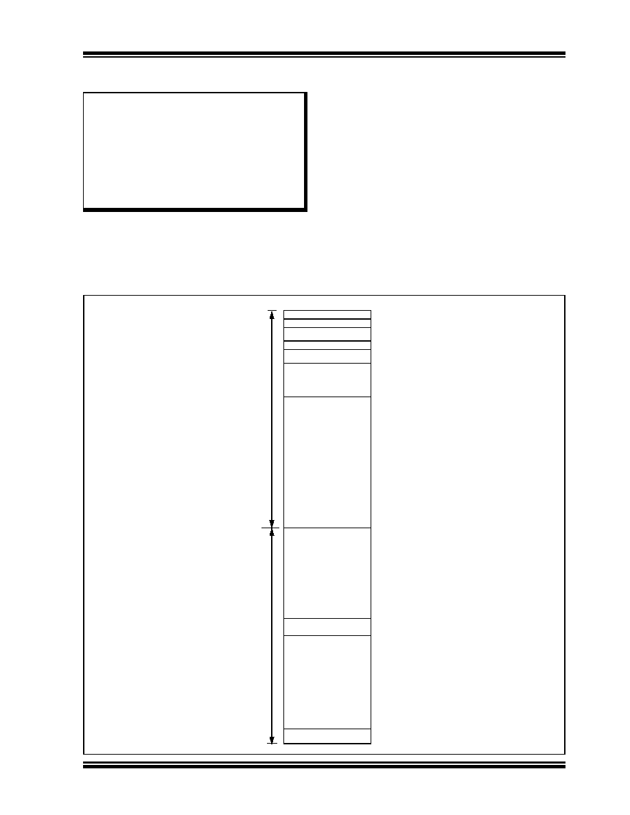
FIGURE 4-1:
PROGRAM MEMORY MAP FOR dsPIC33FJ12MC201/202 DEVICES
Note:
This data sheet summarizes the features
of the dsPIC33FJ12MC201/202 family of
devices. It is not intended to be a
comprehensive reference source. To
complement the information in this data
sheet, refer to Section 4. “Program
Memory”
(DS70202) of the “dsPIC33F/
PIC24H Family Reference Manual”
, which
is available from the Microchip website
(www.microchip.com).
Reset Address
0x000000
0x0000FE
0x000002
0x000100
Device Configuration
User Program
Flash Memory
0x002000
0x001FFE
(4K instructions)
0x800000
0xF80000
Registers
0xF80017
0xF80018
DEVID (2)
0xFEFFFE
0xFF0000
0xFFFFFE
0xF7FFFE
Unimplemented
(Read ‘0’s)
GOTO
Instruction
0x000004
Reserved
0x7FFFFE
Reserved
0x000200
0x0001FE
0x000104
Alternate Vector Table
Reserved
Interrupt Vector Table
dsPIC33FJ12MC201/202
Confi
gur
ati
on
Memory
S
pace
Us
er
Memor
yS
pac
e
相关PDF资料 |
PDF描述 |
|---|---|
| PIC18F67J10T-I/PT | IC PIC MCU FLASH 64KX16 64TQFP |
| ADG509FBRNZ | IC MULTIPLEXER DUAL 4X1 16SOIC |
| PIC16C770T-I/SS | IC MCU OTP 2KX14 A/D PWM 20SSOP |
| PIC16LC711-04E/P | IC MCU OTP 1KX14 A/D 18DIP |
| VE-BNF-CU-F2 | CONVERTER MOD DC/DC 72V 200W |
相关代理商/技术参数 |
参数描述 |
|---|---|
| dsPIC33FJ16GP101-E/P | 功能描述:数字信号处理器和控制器 - DSP, DSC 16bit DSC Fam 16MIPS 16KB FL 1KB RAM RoHS:否 制造商:Microchip Technology 核心:dsPIC 数据总线宽度:16 bit 程序存储器大小:16 KB 数据 RAM 大小:2 KB 最大时钟频率:40 MHz 可编程输入/输出端数量:35 定时器数量:3 设备每秒兆指令数:50 MIPs 工作电源电压:3.3 V 最大工作温度:+ 85 C 封装 / 箱体:TQFP-44 安装风格:SMD/SMT |
| dsPIC33FJ16GP101-E/SO | 功能描述:数字信号处理器和控制器 - DSP, DSC 16bit DSC Fam 16MIPS 16KB FL 1KB RAM RoHS:否 制造商:Microchip Technology 核心:dsPIC 数据总线宽度:16 bit 程序存储器大小:16 KB 数据 RAM 大小:2 KB 最大时钟频率:40 MHz 可编程输入/输出端数量:35 定时器数量:3 设备每秒兆指令数:50 MIPs 工作电源电压:3.3 V 最大工作温度:+ 85 C 封装 / 箱体:TQFP-44 安装风格:SMD/SMT |
| dsPIC33FJ16GP101-E/SS | 功能描述:数字信号处理器和控制器 - DSP, DSC 16bit DSC Fam 16MIPS 16KB FL 1KB RAM RoHS:否 制造商:Microchip Technology 核心:dsPIC 数据总线宽度:16 bit 程序存储器大小:16 KB 数据 RAM 大小:2 KB 最大时钟频率:40 MHz 可编程输入/输出端数量:35 定时器数量:3 设备每秒兆指令数:50 MIPs 工作电源电压:3.3 V 最大工作温度:+ 85 C 封装 / 箱体:TQFP-44 安装风格:SMD/SMT |
| dsPIC33FJ16GP101-I/P | 功能描述:数字信号处理器和控制器 - DSP, DSC 16bit DSC Fam 16MIPS 16KB FL 1KB RAM RoHS:否 制造商:Microchip Technology 核心:dsPIC 数据总线宽度:16 bit 程序存储器大小:16 KB 数据 RAM 大小:2 KB 最大时钟频率:40 MHz 可编程输入/输出端数量:35 定时器数量:3 设备每秒兆指令数:50 MIPs 工作电源电压:3.3 V 最大工作温度:+ 85 C 封装 / 箱体:TQFP-44 安装风格:SMD/SMT |
| dsPIC33FJ16GP101-I/SO | 功能描述:数字信号处理器和控制器 - DSP, DSC 16bit DSC Fam 16MIPS 16KB FL 1KB RAM RoHS:否 制造商:Microchip Technology 核心:dsPIC 数据总线宽度:16 bit 程序存储器大小:16 KB 数据 RAM 大小:2 KB 最大时钟频率:40 MHz 可编程输入/输出端数量:35 定时器数量:3 设备每秒兆指令数:50 MIPs 工作电源电压:3.3 V 最大工作温度:+ 85 C 封装 / 箱体:TQFP-44 安装风格:SMD/SMT |
发布紧急采购,3分钟左右您将得到回复。