- 您现在的位置:买卖IC网 > PDF目录295865 > E28F320J5-120 (INTEL CORP) StrataFlash MEMORY TECHNOLOGY 32 AND 64 MBIT PDF资料下载
参数资料
| 型号: | E28F320J5-120 |
| 厂商: | INTEL CORP |
| 元件分类: | PROM |
| 英文描述: | StrataFlash MEMORY TECHNOLOGY 32 AND 64 MBIT |
| 中文描述: | 2M X 16 FLASH 5V PROM, 150 ns, PDSO56 |
| 封装: | 14 X 20 MM, TSOP-56 |
| 文件页数: | 8/51页 |
| 文件大小: | 651K |
| 代理商: | E28F320J5-120 |
第1页第2页第3页第4页第5页第6页第7页当前第8页第9页第10页第11页第12页第13页第14页第15页第16页第17页第18页第19页第20页第21页第22页第23页第24页第25页第26页第27页第28页第29页第30页第31页第32页第33页第34页第35页第36页第37页第38页第39页第40页第41页第42页第43页第44页第45页第46页第47页第48页第49页第50页第51页
28F320J5 and 28F640J5
16
Datasheet
3.7
Write
Writing commands to the CUI enables reading of device data, query, identifier codes, inspection
and clearing of the status register, and, when VPEN =VPENH, block erasure, program, and lock-bit
configuration.
The Block Erase command requires appropriate command data and an address within the block to
be erased. The Byte/Word Program command requires the command and address of the location to
be written. Set Master and Block Lock-Bit commands require the command and address within the
device (Master Lock) or block within the device (Block Lock) to be locked. The Clear Block Lock-
Bits command requires the command and address within the device.
The CUI does not occupy an addressable memory location. It is written when the device is enabled
and WE# is active. The address and data needed to execute a command are latched on the rising
page 12). Standard microprocessor write timings are used.
NOTES:
1. See Table 2 for valid CE configurations.
2. OE# and WE# should never be enabled simultaneously.
3. DQ refers to DQ0–DQ7 if BYTE# is low and DQ0–DQ15 if BYTE# is high.
4. Refer to DC Characteristics. When VPEN ≤ VPENLK, memory contents can be read, but not altered.
5. X can be VIL or VIH for control and address pins, and VPENLK or VPENH for VPEN.See DC Characteristics for
VPENLK and VPENH voltages.
6. In default mode, STS is VOL when the WSM is executinginternal block erase, program, or lock-bit
configuration algorithms. It is VOH when the WSM is not busy, in block erase suspend mode (with
programming inactive), or reset/power-down mode.
7. High Z will be VOH with an external pull-up resistor.
8. See Read Identifier Codes Command section for read identifier code data.
9. See Read Query Mode Command section for read query data.
10.Command writes involving block erase, program, or lock-bit configuration are reliably executed when VPEN =
VPENH and VCC is within specification. Block erase, program, or lock-bit configuration with VIH <RP# < VHH
produce spurious results and should not be attempted.
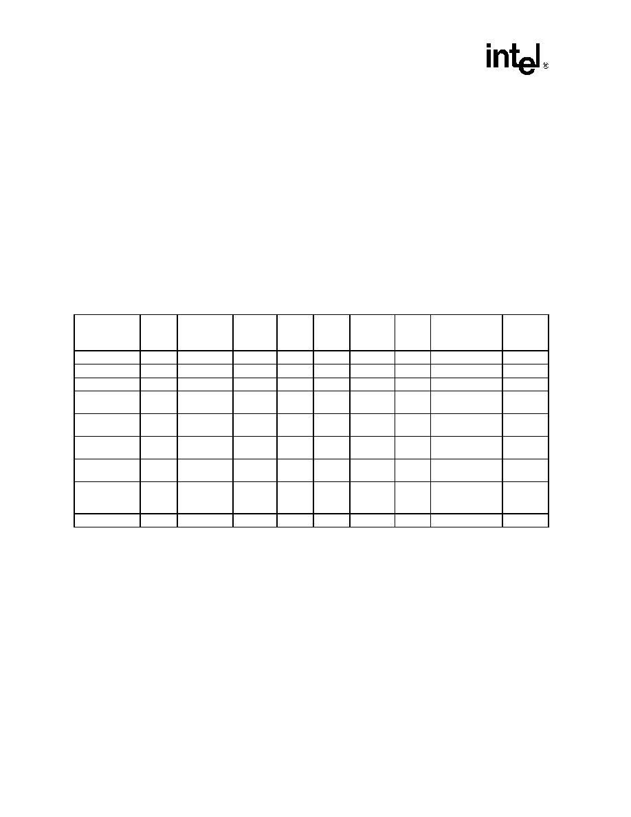
Table 3.
Bus Operations
Mode
Notes
RP#
CE0,1,2
(1)
OE#(2)
WE#(2)
Address
VPEN
DQ(3)
STS
(default
mode)
Read Array
4,5,6
VIH or VHH
Enabled
VIL
VIH
XX
DOUT
High Z(7)
Output Disable
VIH or VHH
Enabled
VIH
XX
High Z
X
Standby
VIH or VHH
Disabled
X
High Z
X
Reset/Power-
Down Mode
VIL
X
HighZ
HighZ(7)
Read Identifier
Codes
VIH or VHH
Enabled
VIL
VIH
See
X
Note8
HighZ(7)
Read Query
VIH or VHH
Enabled
VIL
VIH
See
X
Note9
HighZ(7)
Read Status
(WSM off)
VIH or VHH
Enabled
VIL
VIH
XX
DOUT
Read Status
(WSM on)
VIH or VHH
Enabled
VIL
VIH
XVPENH
DQ7 =DOUT
DQ15–8 =High Z
DQ6–0 =High Z
Write
6,10,11
VIH or VHH
Enabled
VIH
VIL
XX
DIN
X
相关PDF资料 |
PDF描述 |
|---|---|
| E28F400BX-B120 | 4-MBIT (256K X 16, 512K X 8) BOOT BLOCK FLASH MEMORY FAMILY |
| E28F400BX-B60 | ACTUATOR, SWITCH, ROUND, MOMENTARY; Approval Bodies:BEAB, VDE, UL, CSA; Diameter, external:29mm; IP rating:65; Operations, mechanical No. of:1000000; Temp, op. max:85(degree C); Temp, op. min:-20(degree C) RoHS Compliant: Yes |
| E28F400BX-B80 | 4-MBIT (256K X 16, 512K X 8) BOOT BLOCK FLASH MEMORY FAMILY |
| E28F400BX-T120 | 4-MBIT (256K X 16, 512K X 8) BOOT BLOCK FLASH MEMORY FAMILY |
| E28F004BX-T120 | OSC 5V SMT PLAS 14X9 CMOS |
相关代理商/技术参数 |
参数描述 |
|---|---|
| E28F320J5A-120 | 制造商:Intel 功能描述: |
| E28F320S5-110 | 制造商:INTEL 制造商全称:Intel Corporation 功能描述:WORD-WIDE FlashFile MEMORY FAMILY |
| E28F320S5-90 | 制造商:INTEL 制造商全称:Intel Corporation 功能描述:WORD-WIDE FlashFile MEMORY FAMILY |
| E28F400B5B60 | 制造商:INTEL 制造商全称:Intel Corporation 功能描述:SMART 5 BOOT BLOCK FLASH MEMORY FAMILY 2, 4, 8 MBIT |
| E28F400B5B80 | 制造商:Rochester Electronics LLC 功能描述: 制造商:Intel 功能描述: |
发布紧急采购,3分钟左右您将得到回复。