- 您现在的位置:买卖IC网 > PDF目录299030 > EP20K100BC484-2 (ALTERA CORP) LOADABLE PLD, PBGA484 PDF资料下载
参数资料
| 型号: | EP20K100BC484-2 |
| 厂商: | ALTERA CORP |
| 元件分类: | PLD |
| 英文描述: | LOADABLE PLD, PBGA484 |
| 文件页数: | 20/68页 |
| 文件大小: | 975K |
| 代理商: | EP20K100BC484-2 |
第1页第2页第3页第4页第5页第6页第7页第8页第9页第10页第11页第12页第13页第14页第15页第16页第17页第18页第19页当前第20页第21页第22页第23页第24页第25页第26页第27页第28页第29页第30页第31页第32页第33页第34页第35页第36页第37页第38页第39页第40页第41页第42页第43页第44页第45页第46页第47页第48页第49页第50页第51页第52页第53页第54页第55页第56页第57页第58页第59页第60页第61页第62页第63页第64页第65页第66页第67页第68页
27
4317K–AVR–03/2013
AT90PWM2/3/2B/3B
6.4
I/O Memory
The I/O space definition of the AT90PWM2/2B/3/3B is shown in “Register Summary” on page
All AT90PWM2/2B/3/3B I/Os and peripherals are placed in the I/O space. All I/O locations may
be accessed by the LD/LDS/LDD and ST/STS/STD instructions, transferring data between the
32 general purpose working registers and the I/O space. I/O registers within the address range
0x00 - 0x1F are directly bit-accessible using the SBI and CBI instructions. In these registers, the
value of single bits can be checked by using the SBIS and SBIC instructions. Refer to the
instruction set section for more details. When using the I/O specific commands IN and OUT, the
I/O addresses 0x00 - 0x3F must be used. When addressing I/O registers as data space using
LD and ST instructions, 0x20 must be added to these addresses. The AT90PWM2/2B/3/3B is a
complex microcontroller with more peripheral units than can be supported within the 64 location
reserved in Opcode for the IN and OUT instructions. For the Extended I/O space from 0x60 -
0xFF in SRAM, only the ST/STS/STD and LD/LDS/LDD instructions can be used.
For compatibility with future devices, reserved bits should be written to zero if accessed.
Reserved I/O memory addresses should never be written.
Some of the status flags are cleared by writing a logical one to them. Note that, unlike most other
AVR’s, the CBI and SBI instructions will only operate on the specified bit, and can therefore be
used on registers containing such status flags. The CBI and SBI instructions work with registers
0x00 to 0x1F only.
The I/O and peripherals control registers are explained in later sections.
6.5
General Purpose I/O Registers
The AT90PWM2/2B/3/3B contains four General Purpose I/O Registers. These registers can be
used for storing any information, and they are particularly useful for storing global variables and
status flags.
The General Purpose I/O Registers, within the address range 0x00 - 0x1F, are directly bit-
accessible using the SBI, CBI, SBIS, and SBIC instructions.
6.5.1
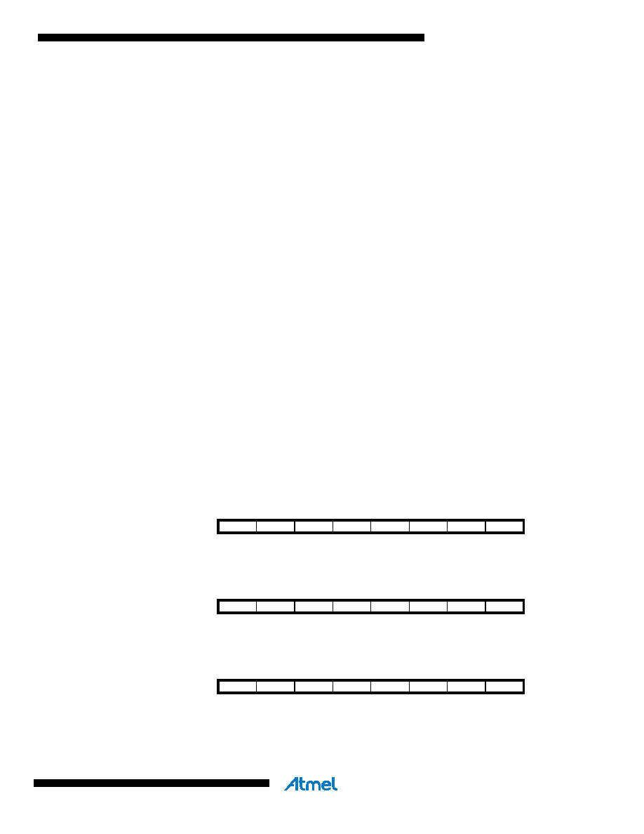
General Purpose I/O Register 0 – GPIOR0
6.5.2
General Purpose I/O Register 1 – GPIOR1
6.5.3
General Purpose I/O Register 2 – GPIOR2
Bit
765
4321
0
GPIOR07 GPIOR06 GPIOR05 GPIOR04 GPIOR03 GPIOR02 GPIOR01 GPIOR00
GPIOR0
Read/Write
R/W
Initial Value
000
0000
0
Bit
765
4321
0
GPIOR17 GPIOR16 GPIOR15 GPIOR14 GPIOR13 GPIOR12 GPIOR11 GPIOR10
GPIOR1
Read/Write
R/W
Initial Value
000
0000
0
Bit
765
4321
0
GPIOR27 GPIOR26 GPIOR25 GPIOR24 GPIOR23 GPIOR22 GPIOR21 GPIOR20
GPIOR2
Read/Write
R/W
Initial Value
000
0000
0
相关PDF资料 |
PDF描述 |
|---|---|
| EP20K100BC484-3 | LOADABLE PLD, PBGA484 |
| EP20K100BI484-1 | LOADABLE PLD, PBGA484 |
| EP20K100BI484-2 | LOADABLE PLD, PBGA484 |
| EP20K100BI484-3 | LOADABLE PLD, PBGA484 |
| EP20K100BC672-1 | LOADABLE PLD, PBGA672 |
相关代理商/技术参数 |
参数描述 |
|---|---|
| EP20K100BI356-1 | 制造商:未知厂家 制造商全称:未知厂家 功能描述:Field Programmable Gate Array (FPGA) |
| EP20K100BI356-1ES | 制造商:未知厂家 制造商全称:未知厂家 功能描述:FPGA |
| EP20K100BI356-2 | 制造商:未知厂家 制造商全称:未知厂家 功能描述:Field Programmable Gate Array (FPGA) |
| EP20K100BI356-2ES | 制造商:未知厂家 制造商全称:未知厂家 功能描述:FPGA |
| EP20K100BI356-3 | 制造商:未知厂家 制造商全称:未知厂家 功能描述:Field Programmable Gate Array (FPGA) |
发布紧急采购,3分钟左右您将得到回复。