- 您现在的位置:买卖IC网 > PDF目录299030 > EP20K100BC484-2 (ALTERA CORP) LOADABLE PLD, PBGA484 PDF资料下载
参数资料
| 型号: | EP20K100BC484-2 |
| 厂商: | ALTERA CORP |
| 元件分类: | PLD |
| 英文描述: | LOADABLE PLD, PBGA484 |
| 文件页数: | 36/68页 |
| 文件大小: | 975K |
| 代理商: | EP20K100BC484-2 |
第1页第2页第3页第4页第5页第6页第7页第8页第9页第10页第11页第12页第13页第14页第15页第16页第17页第18页第19页第20页第21页第22页第23页第24页第25页第26页第27页第28页第29页第30页第31页第32页第33页第34页第35页当前第36页第37页第38页第39页第40页第41页第42页第43页第44页第45页第46页第47页第48页第49页第50页第51页第52页第53页第54页第55页第56页第57页第58页第59页第60页第61页第62页第63页第64页第65页第66页第67页第68页
41
4317K–AVR–03/2013
AT90PWM2/3/2B/3B
8.
Power Management and Sleep Modes
Sleep modes enable the application to shut down unused modules in the MCU, thereby saving
power. The AVR provides various sleep modes allowing the user to tailor the power consump-
tion to the application’s requirements.
To enter any of the five sleep modes, the SE bit in SMCR must be written to logic one and a
SLEEP instruction must be executed. The SM2, SM1, and SM0 bits in the SMCR Register select
which sleep mode (Idle, ADC Noise Reduction, Power-down, Power-save, or Standby) will be
activated by the SLEEP instruction. See Table 8-1 for a summary. If an enabled interrupt occurs
while the MCU is in a sleep mode, the MCU wakes up. The MCU is then halted for four cycles in
addition to the start-up time, executes the interrupt routine, and resumes execution from the
instruction following SLEEP. The contents of the register file and SRAM are unaltered when the
device wakes up from sleep. If a reset occurs during sleep mode, the MCU wakes up and exe-
cutes from the Reset Vector.
Figure 7-1 on page 29 presents the different clock systems in the AT90PWM2/2B/3/3B, and their
distribution. The figure is helpful in selecting an appropriate sleep mode.
8.1
Sleep Mode Control Register – SMCR
The Sleep Mode Control Register contains control bits for power management.
Bits 3..1 – SM2..0: Sleep Mode Select Bits 2, 1, and 0
These bits select between the five available sleep modes as shown in Table 8-1.
Note:
1. Standby mode is only recommended for use with external crystals or resonators.
Bit 1 – SE: Sleep Enable
The SE bit must be written to logic one to make the MCU enter the sleep mode when the SLEEP
instruction is executed. To avoid the MCU entering the sleep mode unless it is the programmer’s
purpose, it is recommended to write the Sleep Enable (SE) bit to one just before the execution of
the SLEEP instruction and to clear it immediately after waking up.
8.2
Idle Mode
When the SM2..0 bits are written to 000, the SLEEP instruction makes the MCU enter Idle
mode, stopping the CPU but allowing SPI, USART, Analog Comparator, ADC, Timer/Counters,
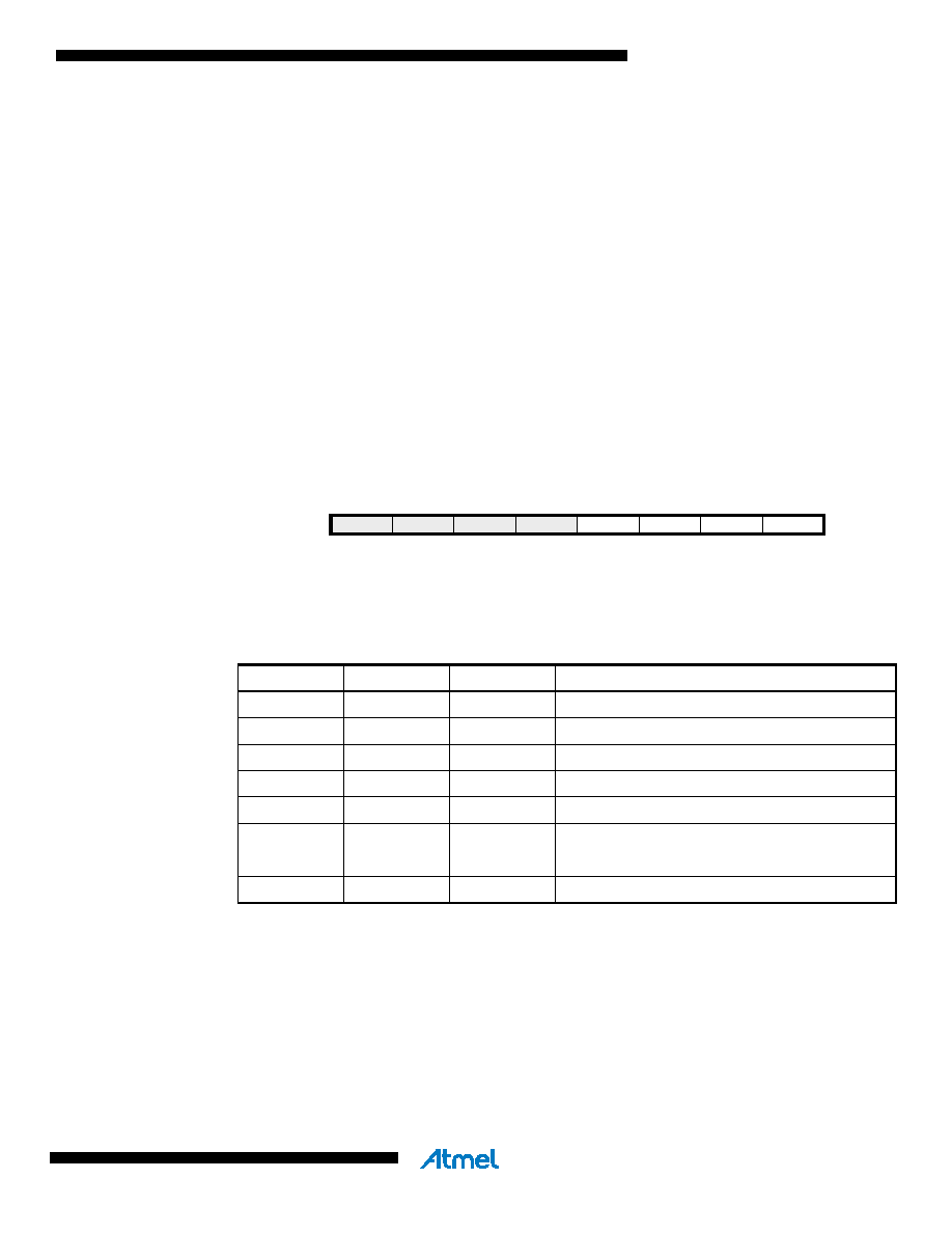
Bit
76543210
–
SM2
SM1
SM0
SE
SMCR
Read/Write
RRRR
R/W
Initial Value
00000000
Table 8-1.
Sleep Mode Select
SM2
SM1
SM0
Sleep Mode
000
Idle
0
1
ADC Noise Reduction
010
Power-down
011
Reserved
100
Reserved
101
Reserved
110
Standby(1)
111
Reserved
相关PDF资料 |
PDF描述 |
|---|---|
| EP20K100BC484-3 | LOADABLE PLD, PBGA484 |
| EP20K100BI484-1 | LOADABLE PLD, PBGA484 |
| EP20K100BI484-2 | LOADABLE PLD, PBGA484 |
| EP20K100BI484-3 | LOADABLE PLD, PBGA484 |
| EP20K100BC672-1 | LOADABLE PLD, PBGA672 |
相关代理商/技术参数 |
参数描述 |
|---|---|
| EP20K100BI356-1 | 制造商:未知厂家 制造商全称:未知厂家 功能描述:Field Programmable Gate Array (FPGA) |
| EP20K100BI356-1ES | 制造商:未知厂家 制造商全称:未知厂家 功能描述:FPGA |
| EP20K100BI356-2 | 制造商:未知厂家 制造商全称:未知厂家 功能描述:Field Programmable Gate Array (FPGA) |
| EP20K100BI356-2ES | 制造商:未知厂家 制造商全称:未知厂家 功能描述:FPGA |
| EP20K100BI356-3 | 制造商:未知厂家 制造商全称:未知厂家 功能描述:Field Programmable Gate Array (FPGA) |
发布紧急采购,3分钟左右您将得到回复。