- 您现在的位置:买卖IC网 > PDF目录19322 > EP2AGX65DF29I3N (Altera)IC ARRIA II GX FPGA 65K 780FBGA PDF资料下载
参数资料
| 型号: | EP2AGX65DF29I3N |
| 厂商: | Altera |
| 文件页数: | 35/90页 |
| 文件大小: | 0K |
| 描述: | IC ARRIA II GX FPGA 65K 780FBGA |
| 产品培训模块: | Three Reasons to Use FPGA's in Industrial Designs |
| 标准包装: | 4 |
| 系列: | Arria II GX |
| LAB/CLB数: | 2530 |
| 逻辑元件/单元数: | 60214 |
| RAM 位总计: | 5371904 |
| 输入/输出数: | 364 |
| 电源电压: | 0.87 V ~ 0.93 V |
| 安装类型: | 表面贴装 |
| 工作温度: | -40°C ~ 100°C |
| 封装/外壳: | 780-BBGA |
| 供应商设备封装: | 780-FBGA(29x29) |
| 其它名称: | 544-2702 |
第1页第2页第3页第4页第5页第6页第7页第8页第9页第10页第11页第12页第13页第14页第15页第16页第17页第18页第19页第20页第21页第22页第23页第24页第25页第26页第27页第28页第29页第30页第31页第32页第33页第34页当前第35页第36页第37页第38页第39页第40页第41页第42页第43页第44页第45页第46页第47页第48页第49页第50页第51页第52页第53页第54页第55页第56页第57页第58页第59页第60页第61页第62页第63页第64页第65页第66页第67页第68页第69页第70页第71页第72页第73页第74页第75页第76页第77页第78页第79页第80页第81页第82页第83页第84页第85页第86页第87页第88页第89页第90页
1–32
Chapter 1: Device Datasheet for Arria II Devices
Switching Characteristics
December 2013
Altera Corporation
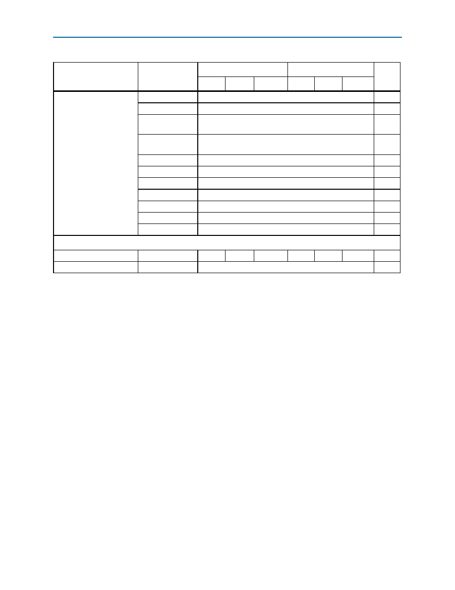
-3 dB Bandwidth
PCIe Gen1
2.5 - 3.5
MHz
PCIe Gen2
6 - 8
MHz
(OIF) CEI PHY at
4.976 Gbps
7 - 11
MHz
(OIF) CEI PHY at
6.375 Gbps
5 - 10
MHz
XAUI
2 - 4
MHz
SRIO 1.25 Gbps
3 - 5.5
MHz
SRIO 2.5 Gbps
3 - 5.5
MHz
SRIO 3.125 Gbps
2 - 4
MHz
GIGE
2.5 - 4.5
MHz
SONET OC12
1.5 - 2.5
MHz
SONET OC48
3.5 - 6
MHz
Transceiver-FPGA Fabric Interface
Interface speed
—
25
—
325
25
—
250
MHz
Digital reset pulse width
—
Minimum is two parallel clock cycles
—
Notes to Table 1–35:
(1) The 3x speed grade is the fastest speed grade offered in the following Arria II GZ devices: EP2AGZ225, EP2AGZ300, and EP2AGZ350.
(2) The rise and fall time transition is specified from 20% to 80%.
(3) To calculate the REFCLK rms phase jitter requirement at reference clock frequencies other than 100 MHz, use the following formula:
REFCLK rms phase jitter at f (MHz) = REFCLK rms phase jitter at 100 MHz * 100/f.
(4) The minimum reconfig_clk frequency is 2.5 MHz if the transceiver channel is configured in Transmitter only mode. The minimum
reconfig_clk
frequency is 37.5 MHz if the transceiver channel is configured in Receiver only or Receiver and Transmitter mode.
(5) If your design uses more than one dynamic reconfiguration controller (altgx_reconfig) instances to control the transceiver (altgx)
channels physically located on the same side of the device AND if you use different reconfig_clk sources for these altgx_reconfig
instances, the delta time between any two of these reconfig_clk sources becoming stable must not exceed the maximum specification listed.
(6) The device cannot tolerate prolonged operation at this absolute maximum.
(7) You must use the 1.1-V RX VICM setting if the input serial data standard is LVDS.
(8) The differential eye opening specification at the receiver input pins assumes that Receiver Equalization is disabled. If you enable Receiver
Equalization, the receiver circuitry can tolerate a lower minimum eye opening, depending on the equalization level. Use H-Spice simulation to
derive the minimum eye opening requirement with Receiver Equalization enabled.
(9) The rate matcher supports only up to
± 300 ppm.
(10) Time taken to rx_pll_locked goes high from rx_analogreset de-assertion. Refer to Figure 1–1 on page 1–33.
(11) Time for which the CDR must be kept in lock-to-reference mode after rx_pll_locked goes high and before rx_locktodata is asserted in
manual mode. Refer to Figure 1–1 on page 1–33.
(12) Time taken to recover valid data after the rx_locktodata signal is asserted in manual mode. Refer to Figure 1–1 on page 1–33.
(13) Time taken to recover valid data after the rx_freqlocked signal goes high in automatic mode. Refer to Figure 1–2 on page 1–33.
(14) A GPLL may be required to meet the PMA-FPGA fabric interface timing above certain data rates. For more information, refer to the Transceiver
(15) The Quartus II software automatically selects the appropriate slew rate depending on the configured data rate or functional mode.
(16) To support data rates lower than the minimum specification through oversampling, use the CDR in LTR mode only.
Table 1–35. Transceiver Specifications for Arria II GZ Devices (Part 5 of 5)
Symbol/
Description
Conditions
–C3 and –I3 (1)
–C4 and –I4
Unit
Min
Typ
Max
Min
Typ
Max
相关PDF资料 |
PDF描述 |
|---|---|
| 1571650-5 | CONN PLUG 9POS SLD CUP 20AWG |
| TAJD108M004RNJ | CAP TANT 1000UF 4V 20% 2917 |
| ASC28DRAH | CONN EDGECARD 56POS .100 R/A DIP |
| VJ1206A200JBBAT4X | CAP CER 20PF 100V 5% NP0 1206 |
| EP2S30F672I4N | IC STRATIX II FPGA 30K 672-FBGA |
相关代理商/技术参数 |
参数描述 |
|---|---|
| EP2AGX65DF29I5 | 功能描述:FPGA - 现场可编程门阵列 FPGA - Arria II GX 2530 LABs 364 IOs RoHS:否 制造商:Altera Corporation 系列:Cyclone V E 栅极数量: 逻辑块数量:943 内嵌式块RAM - EBR:1956 kbit 输入/输出端数量:128 最大工作频率:800 MHz 工作电源电压:1.1 V 最大工作温度:+ 70 C 安装风格:SMD/SMT 封装 / 箱体:FBGA-256 |
| EP2AGX65DF29I5N | 功能描述:FPGA - 现场可编程门阵列 FPGA - Arria II GX 2530 LABs 364 IOs RoHS:否 制造商:Altera Corporation 系列:Cyclone V E 栅极数量: 逻辑块数量:943 内嵌式块RAM - EBR:1956 kbit 输入/输出端数量:128 最大工作频率:800 MHz 工作电源电压:1.1 V 最大工作温度:+ 70 C 安装风格:SMD/SMT 封装 / 箱体:FBGA-256 |
| EP2AGX95DF25C4 | 功能描述:FPGA - 现场可编程门阵列 FPGA - Arria II GX 3747 LABs 260 IOs RoHS:否 制造商:Altera Corporation 系列:Cyclone V E 栅极数量: 逻辑块数量:943 内嵌式块RAM - EBR:1956 kbit 输入/输出端数量:128 最大工作频率:800 MHz 工作电源电压:1.1 V 最大工作温度:+ 70 C 安装风格:SMD/SMT 封装 / 箱体:FBGA-256 |
| EP2AGX95DF25C4N | 功能描述:FPGA - 现场可编程门阵列 FPGA - Arria II GX 3747 LABs 260 IOs RoHS:否 制造商:Altera Corporation 系列:Cyclone V E 栅极数量: 逻辑块数量:943 内嵌式块RAM - EBR:1956 kbit 输入/输出端数量:128 最大工作频率:800 MHz 工作电源电压:1.1 V 最大工作温度:+ 70 C 安装风格:SMD/SMT 封装 / 箱体:FBGA-256 |
| EP2AGX95DF25C5 | 功能描述:FPGA - 现场可编程门阵列 FPGA - Arria II GX 3747 LABs 260 IOs RoHS:否 制造商:Altera Corporation 系列:Cyclone V E 栅极数量: 逻辑块数量:943 内嵌式块RAM - EBR:1956 kbit 输入/输出端数量:128 最大工作频率:800 MHz 工作电源电压:1.1 V 最大工作温度:+ 70 C 安装风格:SMD/SMT 封装 / 箱体:FBGA-256 |
发布紧急采购,3分钟左右您将得到回复。