- 您现在的位置:买卖IC网 > PDF目录19322 > EP2AGX65DF29I3N (Altera)IC ARRIA II GX FPGA 65K 780FBGA PDF资料下载
参数资料
| 型号: | EP2AGX65DF29I3N |
| 厂商: | Altera |
| 文件页数: | 75/90页 |
| 文件大小: | 0K |
| 描述: | IC ARRIA II GX FPGA 65K 780FBGA |
| 产品培训模块: | Three Reasons to Use FPGA's in Industrial Designs |
| 标准包装: | 4 |
| 系列: | Arria II GX |
| LAB/CLB数: | 2530 |
| 逻辑元件/单元数: | 60214 |
| RAM 位总计: | 5371904 |
| 输入/输出数: | 364 |
| 电源电压: | 0.87 V ~ 0.93 V |
| 安装类型: | 表面贴装 |
| 工作温度: | -40°C ~ 100°C |
| 封装/外壳: | 780-BBGA |
| 供应商设备封装: | 780-FBGA(29x29) |
| 其它名称: | 544-2702 |
第1页第2页第3页第4页第5页第6页第7页第8页第9页第10页第11页第12页第13页第14页第15页第16页第17页第18页第19页第20页第21页第22页第23页第24页第25页第26页第27页第28页第29页第30页第31页第32页第33页第34页第35页第36页第37页第38页第39页第40页第41页第42页第43页第44页第45页第46页第47页第48页第49页第50页第51页第52页第53页第54页第55页第56页第57页第58页第59页第60页第61页第62页第63页第64页第65页第66页第67页第68页第69页第70页第71页第72页第73页第74页当前第75页第76页第77页第78页第79页第80页第81页第82页第83页第84页第85页第86页第87页第88页第89页第90页
Chapter 1: Device Datasheet for Arria II Devices
1–69
Switching Characteristics
December 2013
Altera Corporation
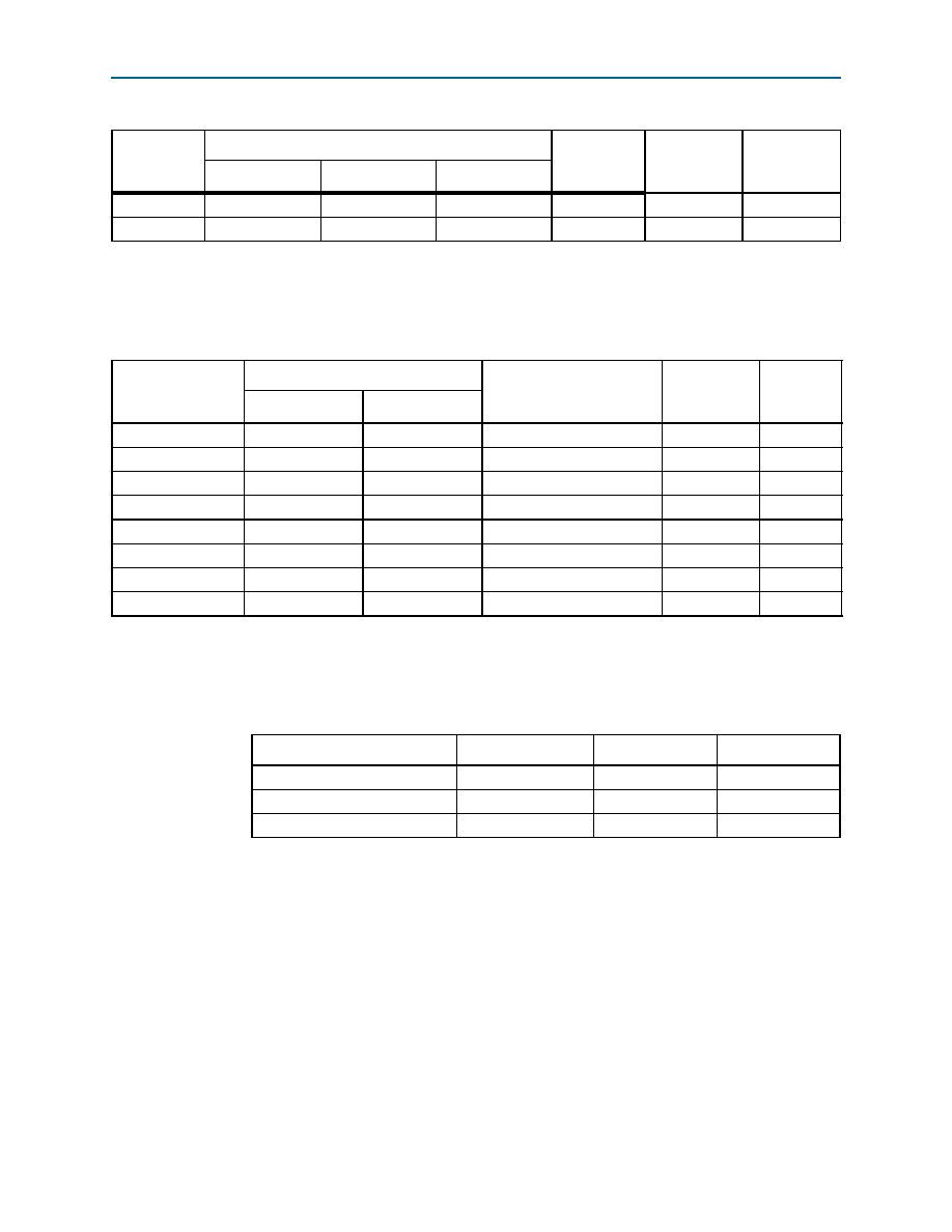
Table 1–58 lists the DLL frequency range specifications for Arria II GZ devices.
Table 1–59 lists the DQS phase offset delay per stage for Arria II GX devices.
5
270-410
270-380
270-320
36
High
10
6
320-450
320-410
320-370
45
High
8
Note to Table 1–57:
(1) Low indicates a 6-bit DQS delay setting; high indicates a 5-bit DQS delay setting.
Table 1–57. External Memory Interface Specifications for Arria II GX Devices (Part 2 of 2)
Frequency
Mode
Frequency Range (MHz)
Resolution
(°)
DQS Delay
Buffer Mode
(1)
Number of
Delay Chains
C4
I3, C5, I5
C6
Table 1–58. DLL Frequency Range Specifications for Arria II GZ Devices
Frequency Mode
Frequency Range (MHz)
Available Phase Shift
DQS Delay
Buffer Mode
Number of
Delay
Chains
–3
–4
0
90-130
90-120
22.5°, 45°, 67.5°, 90°
Low
16
1
120-170
120-160
30°, 60°, 90°, 120°
Low
12
2
150-210
150-200
36°, 72°, 108°, 144°
Low
10
3
180-260
180-240
45°, 90°,135°, 180°
Low
8
4
240-320
240-290
30°, 60°, 90°, 120°
High
12
5
290-380
290-360
36°, 72°, 108°, 144°
High
10
6
360-450
45°, 90°, 135°, 180°
High
8
7
470-630
470-590
60°, 120°, 180°, 240°
High
6
Note to Table 1–58:
(1) Low indicates a 6-bit DQS delay setting; high indicates a 5-bit DQS delay setting.
Speed Grade
Min
Max
Unit
C4
7.0
13.0
ps
I3, C5, I5
7.0
15.0
ps
C6
8.5
18.0
ps
Notes to Table 1–59:
(1) The valid settings for phase offset are -64 to +63 for frequency modes 0 to 3 and -32 to +31 for frequency modes
4 to 5.
(2) The typical value equals the average of the minimum and maximum values.
(3) The delay settings are linear.
相关PDF资料 |
PDF描述 |
|---|---|
| 1571650-5 | CONN PLUG 9POS SLD CUP 20AWG |
| TAJD108M004RNJ | CAP TANT 1000UF 4V 20% 2917 |
| ASC28DRAH | CONN EDGECARD 56POS .100 R/A DIP |
| VJ1206A200JBBAT4X | CAP CER 20PF 100V 5% NP0 1206 |
| EP2S30F672I4N | IC STRATIX II FPGA 30K 672-FBGA |
相关代理商/技术参数 |
参数描述 |
|---|---|
| EP2AGX65DF29I5 | 功能描述:FPGA - 现场可编程门阵列 FPGA - Arria II GX 2530 LABs 364 IOs RoHS:否 制造商:Altera Corporation 系列:Cyclone V E 栅极数量: 逻辑块数量:943 内嵌式块RAM - EBR:1956 kbit 输入/输出端数量:128 最大工作频率:800 MHz 工作电源电压:1.1 V 最大工作温度:+ 70 C 安装风格:SMD/SMT 封装 / 箱体:FBGA-256 |
| EP2AGX65DF29I5N | 功能描述:FPGA - 现场可编程门阵列 FPGA - Arria II GX 2530 LABs 364 IOs RoHS:否 制造商:Altera Corporation 系列:Cyclone V E 栅极数量: 逻辑块数量:943 内嵌式块RAM - EBR:1956 kbit 输入/输出端数量:128 最大工作频率:800 MHz 工作电源电压:1.1 V 最大工作温度:+ 70 C 安装风格:SMD/SMT 封装 / 箱体:FBGA-256 |
| EP2AGX95DF25C4 | 功能描述:FPGA - 现场可编程门阵列 FPGA - Arria II GX 3747 LABs 260 IOs RoHS:否 制造商:Altera Corporation 系列:Cyclone V E 栅极数量: 逻辑块数量:943 内嵌式块RAM - EBR:1956 kbit 输入/输出端数量:128 最大工作频率:800 MHz 工作电源电压:1.1 V 最大工作温度:+ 70 C 安装风格:SMD/SMT 封装 / 箱体:FBGA-256 |
| EP2AGX95DF25C4N | 功能描述:FPGA - 现场可编程门阵列 FPGA - Arria II GX 3747 LABs 260 IOs RoHS:否 制造商:Altera Corporation 系列:Cyclone V E 栅极数量: 逻辑块数量:943 内嵌式块RAM - EBR:1956 kbit 输入/输出端数量:128 最大工作频率:800 MHz 工作电源电压:1.1 V 最大工作温度:+ 70 C 安装风格:SMD/SMT 封装 / 箱体:FBGA-256 |
| EP2AGX95DF25C5 | 功能描述:FPGA - 现场可编程门阵列 FPGA - Arria II GX 3747 LABs 260 IOs RoHS:否 制造商:Altera Corporation 系列:Cyclone V E 栅极数量: 逻辑块数量:943 内嵌式块RAM - EBR:1956 kbit 输入/输出端数量:128 最大工作频率:800 MHz 工作电源电压:1.1 V 最大工作温度:+ 70 C 安装风格:SMD/SMT 封装 / 箱体:FBGA-256 |
发布紧急采购,3分钟左右您将得到回复。