- 您现在的位置:买卖IC网 > PDF目录299032 > EPF6024AFC256-2 (ALTERA CORP) LOADABLE PLD, PBGA256 PDF资料下载
参数资料
| 型号: | EPF6024AFC256-2 |
| 厂商: | ALTERA CORP |
| 元件分类: | PLD |
| 英文描述: | LOADABLE PLD, PBGA256 |
| 封装: | FINE LINE, BGA-256 |
| 文件页数: | 21/57页 |
| 文件大小: | 508K |
| 代理商: | EPF6024AFC256-2 |
第1页第2页第3页第4页第5页第6页第7页第8页第9页第10页第11页第12页第13页第14页第15页第16页第17页第18页第19页第20页当前第21页第22页第23页第24页第25页第26页第27页第28页第29页第30页第31页第32页第33页第34页第35页第36页第37页第38页第39页第40页第41页第42页第43页第44页第45页第46页第47页第48页第49页第50页第51页第52页第53页第54页第55页第56页第57页
28
Altera Corporation
FLEX 6000 Programmable Logic Device Family Data Sheet
Open-drain output pins on 5.0-V or 3.3-V FLEX 6000 devices (with a pull-
up resistor to the 5.0-V supply) can drive 5.0-V CMOS input pins that
require a VIH of 3.5 V. When the open-drain pin is active, it will drive low.
When the pin is inactive, the trace will be pulled up to 5.0 V by the resistor.
The open-drain pin will only drive low or tri-state; it will never drive high.
The rise time is dependent on the value of the pull-up resistor and load
impedance. The IOL current specification should be considered when
selecting a pull-up resistor.
Output pins on 5.0-V FLEX 6000 devices with VCCIO = 3.3 V or 5.0 V (with
a pull-up resistor to the 5.0-V supply) can also drive 5.0-V CMOS input
pins. In this case, the pull-up transistor will turn off when the pin voltage
exceeds 3.3 V. Therefore, the pin does not have to be open-drain.
Power Sequencing & Hot-Socketing
Because FLEX 6000 family devices can be used in a mixed-voltage
environment, they have been designed specifically to tolerate any possible
power-up sequence. The VCCIO and VCCINT power planes can be powered
in any order.
Signals can be driven into 3.3-V FLEX 6000 devices before and during
power up without damaging the device. Additionally, FLEX 6000 devices
do not drive out during power up. Once operating conditions are reached,
FLEX 6000 devices operate as specified by the user.
IEEE Std.
1149.1 (JTAG)
Boundary-Scan
Support
All FLEX 6000 devices provide JTAG BST circuitry that comply with the
IEEE Std. 1149.1-1990 specification. Table 8 shows JTAG instructions for
FLEX 6000 devices. JTAG BST can be performed before or after
configuration, but not during configuration (except when you disable
JTAG support in user mode).
1
See Application Note 39 (IEEE 1149.1 (JTAG) Boundary-Scan
Testing in Altera Devices) for more information on JTAG BST
circuitry.
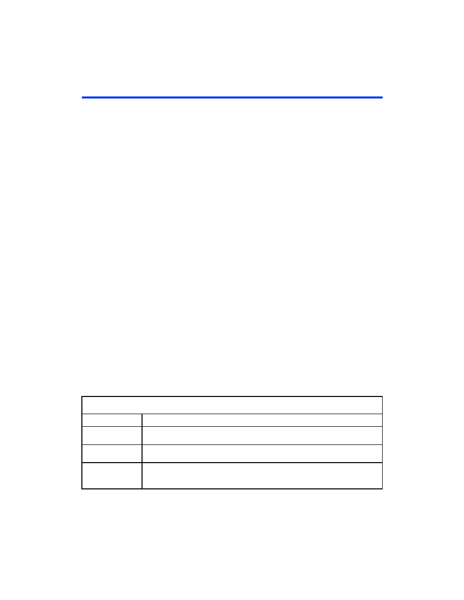
Table 8. FLEX 6000 JTAG Instructions
JTAG Instruction
Description
SAMPLE/PRELOAD Allows a snapshot of the signals at the device pins to be captured and examined during
normal device operation, and permits an initial data pattern to be output at the device pins.
EXTEST
Allows the external circuitry and board-level interconnections to be tested by forcing a test
pattern at the output pins and capturing test result at the input pins.
BYPASS
Places the 1-bit bypass register between the TDI and TDO pins, which allows the BST
data to pass synchronously through the selected device to adjacent devices during
normal device operation.
相关PDF资料 |
PDF描述 |
|---|---|
| EPF6024AFI256-2 | LOADABLE PLD, PBGA256 |
| EPF6024AFC256-3 | LOADABLE PLD, PBGA256 |
| EPL2010-102MLB | Power inductor, shielded, 20% tol, SMT, RoHS |
| EPL2010-102MLC | Power inductor, shielded, 20% tol, SMT, RoHS |
| EPL2010-103MLB | Power inductor, shielded, 20% tol, SMT, RoHS |
相关代理商/技术参数 |
参数描述 |
|---|---|
| EPF6024AFC256-2AA | 制造商:Rochester Electronics LLC 功能描述:- Bulk |
| EPF6024AFC256-3 | 功能描述:FPGA - 现场可编程门阵列 FPGA - Flex 6000 196 LABs 219 IOs RoHS:否 制造商:Altera Corporation 系列:Cyclone V E 栅极数量: 逻辑块数量:943 内嵌式块RAM - EBR:1956 kbit 输入/输出端数量:128 最大工作频率:800 MHz 工作电源电压:1.1 V 最大工作温度:+ 70 C 安装风格:SMD/SMT 封装 / 箱体:FBGA-256 |
| EPF6024AFI256-2 | 功能描述:IC FLEX 6000 FPGA 24K 256-FBGA RoHS:否 类别:集成电路 (IC) >> 嵌入式 - FPGA(现场可编程门阵列) 系列:FLEX 6000 产品变化通告:XC4000(E,L) Discontinuation 01/April/2002 标准包装:24 系列:XC4000E/X LAB/CLB数:100 逻辑元件/单元数:238 RAM 位总计:3200 输入/输出数:80 门数:3000 电源电压:4.5 V ~ 5.5 V 安装类型:表面贴装 工作温度:-40°C ~ 100°C 封装/外壳:120-BCBGA 供应商设备封装:120-CPGA(34.55x34.55) |
| EPF6024AQC208-1 | 功能描述:FPGA - 现场可编程门阵列 FPGA - Flex 6000 196 LABs 171 IOs RoHS:否 制造商:Altera Corporation 系列:Cyclone V E 栅极数量: 逻辑块数量:943 内嵌式块RAM - EBR:1956 kbit 输入/输出端数量:128 最大工作频率:800 MHz 工作电源电压:1.1 V 最大工作温度:+ 70 C 安装风格:SMD/SMT 封装 / 箱体:FBGA-256 |
| EPF6024AQC208-1N | 功能描述:FPGA - 现场可编程门阵列 FPGA - Flex 6000 196 LABs 171 IOs RoHS:否 制造商:Altera Corporation 系列:Cyclone V E 栅极数量: 逻辑块数量:943 内嵌式块RAM - EBR:1956 kbit 输入/输出端数量:128 最大工作频率:800 MHz 工作电源电压:1.1 V 最大工作温度:+ 70 C 安装风格:SMD/SMT 封装 / 箱体:FBGA-256 |
发布紧急采购,3分钟左右您将得到回复。