- 您现在的位置:买卖IC网 > PDF目录17056 > EVAL-AD7322CBZ (Analog Devices Inc)BOARD EVALUATION FOR AD7322 PDF资料下载
参数资料
| 型号: | EVAL-AD7322CBZ |
| 厂商: | Analog Devices Inc |
| 文件页数: | 10/37页 |
| 文件大小: | 0K |
| 描述: | BOARD EVALUATION FOR AD7322 |
| 标准包装: | 1 |
| 系列: | iCMOS® |
| ADC 的数量: | 1 |
| 位数: | 12 |
| 采样率(每秒): | 1M |
| 数据接口: | 串行 |
| 输入范围: | ±10 V |
| 在以下条件下的电源(标准): | 30mW @ 1MSPS |
| 工作温度: | -40°C ~ 85°C |
| 已用 IC / 零件: | AD7322 |
| 已供物品: | 板,CD |
| 相关产品: | AD7322BRUZ-REEL-ND - IC ADC 12BIT+SAR 2CHAN 14-TSSOP AD7322BRUZ-REEL7-ND - IC ADC 12BIT+ SAR 2CHAN 14TSSOP AD7322BRUZ-ND - IC ADC 12BIT+ SAR 2CHAN 14TSSOP |
第1页第2页第3页第4页第5页第6页第7页第8页第9页当前第10页第11页第12页第13页第14页第15页第16页第17页第18页第19页第20页第21页第22页第23页第24页第25页第26页第27页第28页第29页第30页第31页第32页第33页第34页第35页第36页第37页
Data Sheet
AD7322
Rev. B | Page 17 of 36
D
VDD
C2
R1
VIN+
VSS
C1
D
VDD
C2
R1
VIN–
VSS
C1
04863-
024
NOTES
1. VIN+ REFERS TO VIN0 AND VIN– REFERS TO VIN1.
Figure 30. Equivalent Analog Input Circuit (Differential)
Care should be taken to ensure that the analog input does not
exceed the VDD and VSS supply rails by more than 300 mV.
Exceeding this value causes the diodes to become forward
biased and to start conducting into either the VDD supply rail or
VSS supply rail. These diodes can conduct up to 10 mA without
causing irreversible damage to the part.
In Figure 29 and Figure 30, Capacitor C1 is typically 4 pF and
can primarily be attributed to pin capacitance. Resistor R1 is a
lumped component made up of the on resistance of the input
multiplexer and the track-and-hold switch. Capacitor C2 is the
sampling capacitor; its capacitance varies depending on the
analog input range selected (see the Specifications section).
Track-and-Hold Section
The track-and-hold on the analog input of the AD7322 allows
the ADC to accurately convert an input sine wave of full-scale
amplitude to 13-bit accuracy. The input bandwidth of the track-
and-hold is greater than the Nyquist rate of the ADC. The
AD7322 can handle frequencies up to 22 MHz.
The track-and-hold enters its tracking mode on the 14th SCLK
rising edge after the CS falling edge. The time required to acquire
an input signal depends on how quickly the sampling capacitor
is charged. With zero source impedance, 305 ns is sufficient to
acquire the signal to the 13-bit level. The acquisition time
required is calculated using the following formula:
tACQ = 10 × ((RSOURCE + R) C)
where C is the sampling capacitance and R is the resistance seen
by the track-and-hold amplifier looking back on the input.
For the AD7322, the value of R includes the on resistance of the
input multiplexer and is typically 300 . RSOURCE should include
any extra source impedance on the analog input.
When running the AD7322 at a throughput rate of 1 MSPS with
a 20 MHz SCLK signal, the ADC has approximately
1.5 SCLK + t8 + tQUIET
to acquire the analog input signal. The ADC goes back into
hold mode on the CS falling edge.
As the VDD/VSS supply voltage is reduced, the on resistance of
the input multiplexer increases. Therefore, based on the equation
for tACQ, it is necessary to increase the amount of acquisition
time provided to the AD7322 and, therefore, decrease the
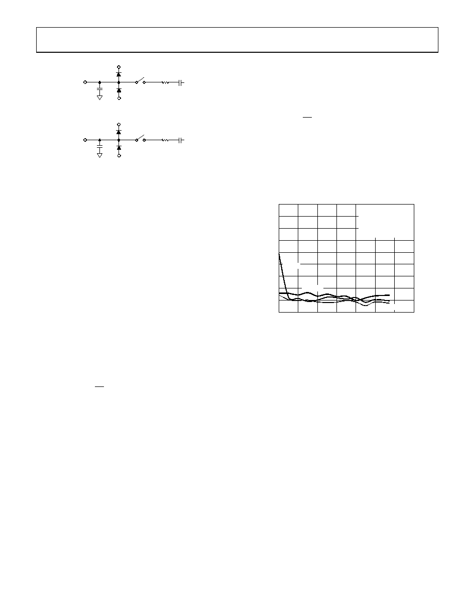
overall throughput rate. Figure 31 shows that if the throughput
rate is reduced when operating with minimum VDD and VSS
supplies, the specified THD performance is maintained.
–50
–95
5
19
±VDD/VSS SUPPLIES (V)
T
HD
(
d
B)
–55
–60
–65
–70
–75
–80
–85
–90
7
9
11
13
15
17
500kSPS
750kSPS
1MSPS
VCC = VDRIVE = 5V
INTERNAL REFERENCE
TA = 25°C
fIN = 10kHz
±5V RANGE
SE MODE
04863-
051
Figure 31. THD vs. ±VDD/VSS Supply Voltage at 500 kSPS, 750 kSPS, and 1 MSPS
Unlike other bipolar ADCs, the AD7322 does not have a
resistive analog input structure. On the AD7322, the bipolar
analog signal is sampled directly onto the sampling capacitor.
This gives the AD7322 high analog input impedance. An
approximation for the analog input impedance can be
calculated from the following formula:
Z = 1/(fS × CS)
where fS is the sampling frequency, and CS is the sampling
capacitor value.
CS depends on the analog input range chosen (see the
Specifications section). When operating at 1 MSPS, the analog
input impedance is typically 75 kΩ for the ±10 V range. As the
sampling frequency is reduced, the analog input impedance
further increases. As the analog input impedance increases, the
current required to drive the analog input therefore decreases.
相关PDF资料 |
PDF描述 |
|---|---|
| EEM31DTMS | CONN EDGECARD 62POS R/A .156 SLD |
| 0210490887 | CABLE JUMPER 1.25MM .152M 19POS |
| GEM30DRMI | CONN EDGECARD 60POS .156 SQ WW |
| EEM28DTKH | CONN EDGECARD 56POS DIP .156 SLD |
| EVAL-AD7484CBZ | BOARD EVALUATION FOR AD7484 |
相关代理商/技术参数 |
参数描述 |
|---|---|
| EVAL-AD7323CB | 制造商:AD 制造商全称:Analog Devices 功能描述:500 kSPS, 4-Channel, Software-Selectable, True Bipolar Input, 12-Bit Plus Sign ADC |
| EVAL-AD7323CBZ | 功能描述:BOARD EVALUATION FOR AD7323CBZ RoHS:是 类别:编程器,开发系统 >> 评估板 - 模数转换器 (ADC) 系列:iCMOS® 产品培训模块:Obsolescence Mitigation Program 标准包装:1 系列:- ADC 的数量:1 位数:12 采样率(每秒):94.4k 数据接口:USB 输入范围:±VREF/2 在以下条件下的电源(标准):- 工作温度:-40°C ~ 85°C 已用 IC / 零件:MAX11645 已供物品:板,软件 |
| EVAL-AD7324CB | 制造商:AD 制造商全称:Analog Devices 功能描述:4-Channel, Software-Selectable, True Bipolar Input, 12-Bit Plus Sign ADC |
| EVAL-AD7324CBZ | 功能描述:BOARD EVALUATION FOR AD7324CBZ RoHS:是 类别:编程器,开发系统 >> 评估板 - 模数转换器 (ADC) 系列:iCMOS® 产品培训模块:Obsolescence Mitigation Program 标准包装:1 系列:- ADC 的数量:1 位数:12 采样率(每秒):94.4k 数据接口:USB 输入范围:±VREF/2 在以下条件下的电源(标准):- 工作温度:-40°C ~ 85°C 已用 IC / 零件:MAX11645 已供物品:板,软件 |
| EVAL-AD7327CB | 制造商:AD 制造商全称:Analog Devices 功能描述:500 kSPS, 8-Channel, Software-Selectable, True Bipolar Input, 12-Bit Plus Sign ADC |
发布紧急采购,3分钟左右您将得到回复。