- 您现在的位置:买卖IC网 > PDF目录17056 > EVAL-AD7322CBZ (Analog Devices Inc)BOARD EVALUATION FOR AD7322 PDF资料下载
参数资料
| 型号: | EVAL-AD7322CBZ |
| 厂商: | Analog Devices Inc |
| 文件页数: | 9/37页 |
| 文件大小: | 0K |
| 描述: | BOARD EVALUATION FOR AD7322 |
| 标准包装: | 1 |
| 系列: | iCMOS® |
| ADC 的数量: | 1 |
| 位数: | 12 |
| 采样率(每秒): | 1M |
| 数据接口: | 串行 |
| 输入范围: | ±10 V |
| 在以下条件下的电源(标准): | 30mW @ 1MSPS |
| 工作温度: | -40°C ~ 85°C |
| 已用 IC / 零件: | AD7322 |
| 已供物品: | 板,CD |
| 相关产品: | AD7322BRUZ-REEL-ND - IC ADC 12BIT+SAR 2CHAN 14-TSSOP AD7322BRUZ-REEL7-ND - IC ADC 12BIT+ SAR 2CHAN 14TSSOP AD7322BRUZ-ND - IC ADC 12BIT+ SAR 2CHAN 14TSSOP |
第1页第2页第3页第4页第5页第6页第7页第8页当前第9页第10页第11页第12页第13页第14页第15页第16页第17页第18页第19页第20页第21页第22页第23页第24页第25页第26页第27页第28页第29页第30页第31页第32页第33页第34页第35页第36页第37页
AD7322
Data Sheet
Rev. B | Page 16 of 36
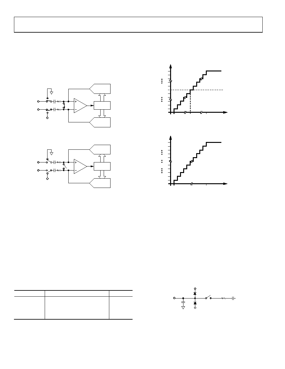
Figure 25 shows the differential configuration during the
acquisition phase. For the conversion phase, SW3 opens and
SW1 and SW2 move to Position B (see Figure 26). The output
impedances of the source driving the VIN+ and VIN pins must
be matched; otherwise, the two inputs will have different
settling times, resulting in errors.
04863-
019
CAPACITIVE
DAC
CONTROL
LOGIC
CAPACITIVE
DAC
COMPARATOR
SW3
SW1
A
B
CS
VIN+
SW2
A
B
VIN–
VREF
NOTES
1. VIN+ REFERS TO VIN0 AND VIN– REFERS TO VIN1.
Figure 25. ADC Differential Configuration During Acquisition Phase
CAPACITIVE
DAC
CONTROL
LOGIC
CAPACITIVE
DAC
COMPARATOR
SW3
SW1
A
B
CS
VIN+
SW2
A
B
VIN–
VREF
04863-
020
NOTES
1. VIN+ REFERS TO VIN0 AND VIN– REFERS TO VIN1.
Figure 26. ADC Differential Configuration During Conversion Phase
Output Coding
The AD7322 default output coding is set to twos complement.
The output coding is controlled by the coding bit in the control
register. To change the output coding to straight binary coding,
the coding bit in the control register must be set. When operat-
ing in sequence mode, the output coding for each channel in
the sequence is the value written to the coding bit during the
last write to the control register.
Transfer Functions
The designed code transitions occur at successive integer
LSB values (that is, 1 LSB, 2 LSB, and so on). The LSB size is
dependent on the analog input range selected.
Table 7. LSB Sizes for Each Analog Input Range
Input Range
Full-Scale Range/8192 Codes
LSB Size
±10 V
20 V
2.441 mV
±5 V
10 V
1.22 mV
±2.5 V
5 V
0.61 mV
0 V to +10 V
10 V
1.22 mV
The ideal transfer characteristic for the AD7322 when twos
complement coding is selected is shown in Figure 27. The ideal
transfer characteristic for the AD7322 when straight binary
coding is selected is shown in Figure 28.
011...111
011...110
000...001
000...000
111...111
–FSR/2 + 1LSB
AGND + 1LSB
+FSR/2 – 1LSB BIPOLAR RANGES
+FSR – 1LSB
UNIPOLAR RANGE
AGND – 1LSB
ANALOG INPUT
ADC
CO
DE
100...010
100...001
100...000
04863-
021
Figure 27. Twos Complement Transfer Characteristic (Bipolar Ranges)
111...111
111...110
111...000
011...111
–FSR/2 + 1LSB
AGND + 1LSB
+FSR/2 – 1LSB BIPOLAR RANGES
+FSR – 1LSB
UNIPOLAR RANGE
ANALOG INPUT
ADC
CO
DE
000...010
000...001
000...000
04863-
022
Figure 28. Straight Binary Transfer Characteristic (Bipolar Ranges)
ANALOG INPUT STRUCTURE
The analog inputs of the AD7322 can be configured as single-
ended, true differential, or pseudo differential via the control
register mode bits (see Table 10). The AD7322 can accept true
bipolar input signals. On power-up, the analog inputs operate as
two single-ended analog input channels. If true differential or
pseudo differential is required, a write to the control register is
necessary after power-up to change this configuration.
Figure 29 shows the equivalent analog input circuit of the
AD7322 in single-ended mode. Figure 30 shows the equivalent
analog input structure in differential mode. The two diodes
provide ESD protection for the analog inputs.
D
VDD
C2
R1
VIN0
VSS
C1
04863-
023
Figure 29. Equivalent Analog Input Circuit (Single-Ended)
相关PDF资料 |
PDF描述 |
|---|---|
| EEM31DTMS | CONN EDGECARD 62POS R/A .156 SLD |
| 0210490887 | CABLE JUMPER 1.25MM .152M 19POS |
| GEM30DRMI | CONN EDGECARD 60POS .156 SQ WW |
| EEM28DTKH | CONN EDGECARD 56POS DIP .156 SLD |
| EVAL-AD7484CBZ | BOARD EVALUATION FOR AD7484 |
相关代理商/技术参数 |
参数描述 |
|---|---|
| EVAL-AD7323CB | 制造商:AD 制造商全称:Analog Devices 功能描述:500 kSPS, 4-Channel, Software-Selectable, True Bipolar Input, 12-Bit Plus Sign ADC |
| EVAL-AD7323CBZ | 功能描述:BOARD EVALUATION FOR AD7323CBZ RoHS:是 类别:编程器,开发系统 >> 评估板 - 模数转换器 (ADC) 系列:iCMOS® 产品培训模块:Obsolescence Mitigation Program 标准包装:1 系列:- ADC 的数量:1 位数:12 采样率(每秒):94.4k 数据接口:USB 输入范围:±VREF/2 在以下条件下的电源(标准):- 工作温度:-40°C ~ 85°C 已用 IC / 零件:MAX11645 已供物品:板,软件 |
| EVAL-AD7324CB | 制造商:AD 制造商全称:Analog Devices 功能描述:4-Channel, Software-Selectable, True Bipolar Input, 12-Bit Plus Sign ADC |
| EVAL-AD7324CBZ | 功能描述:BOARD EVALUATION FOR AD7324CBZ RoHS:是 类别:编程器,开发系统 >> 评估板 - 模数转换器 (ADC) 系列:iCMOS® 产品培训模块:Obsolescence Mitigation Program 标准包装:1 系列:- ADC 的数量:1 位数:12 采样率(每秒):94.4k 数据接口:USB 输入范围:±VREF/2 在以下条件下的电源(标准):- 工作温度:-40°C ~ 85°C 已用 IC / 零件:MAX11645 已供物品:板,软件 |
| EVAL-AD7327CB | 制造商:AD 制造商全称:Analog Devices 功能描述:500 kSPS, 8-Channel, Software-Selectable, True Bipolar Input, 12-Bit Plus Sign ADC |
发布紧急采购,3分钟左右您将得到回复。