- 您现在的位置:买卖IC网 > PDF目录17056 > EVAL-AD7322CBZ (Analog Devices Inc)BOARD EVALUATION FOR AD7322 PDF资料下载
参数资料
| 型号: | EVAL-AD7322CBZ |
| 厂商: | Analog Devices Inc |
| 文件页数: | 26/37页 |
| 文件大小: | 0K |
| 描述: | BOARD EVALUATION FOR AD7322 |
| 标准包装: | 1 |
| 系列: | iCMOS® |
| ADC 的数量: | 1 |
| 位数: | 12 |
| 采样率(每秒): | 1M |
| 数据接口: | 串行 |
| 输入范围: | ±10 V |
| 在以下条件下的电源(标准): | 30mW @ 1MSPS |
| 工作温度: | -40°C ~ 85°C |
| 已用 IC / 零件: | AD7322 |
| 已供物品: | 板,CD |
| 相关产品: | AD7322BRUZ-REEL-ND - IC ADC 12BIT+SAR 2CHAN 14-TSSOP AD7322BRUZ-REEL7-ND - IC ADC 12BIT+ SAR 2CHAN 14TSSOP AD7322BRUZ-ND - IC ADC 12BIT+ SAR 2CHAN 14TSSOP |
第1页第2页第3页第4页第5页第6页第7页第8页第9页第10页第11页第12页第13页第14页第15页第16页第17页第18页第19页第20页第21页第22页第23页第24页第25页当前第26页第27页第28页第29页第30页第31页第32页第33页第34页第35页第36页第37页
Data Sheet
AD7322
Rev. B | Page 31 of 36
MICROPROCESSOR INTERFACING
The serial interface on the AD7322 allows the part to be directly
connected to a range of different microprocessors. This section
explains how to interface the AD7322 with some common micro-
controller and DSP serial interface protocols.
The ADSP-21xx family of DSPs interface directly to the AD7322
the same supply voltage as that of the ADSP-21xx. This allows
the ADC to operate at a higher supply voltage than its serial
interface. The SPORT0 on the ADSP-21xx should be configured
as shown in Table 14.
Table 14. SPORT0 Control Register Setup
Setting
Description
TFSW = RFSW = 1
Alternative framing
INVRFS = INVTFS = 1
Active low frame signal
DTYPE = 00
Right justify data
SLEN = 1111
16-bit data word
ISCLK = 1
Internal serial clock
TFSR = RFSR = 1
Frame every word
IRFS = 0
Internal receive frame sync
ITFS = 1
Internal transmit frame sync
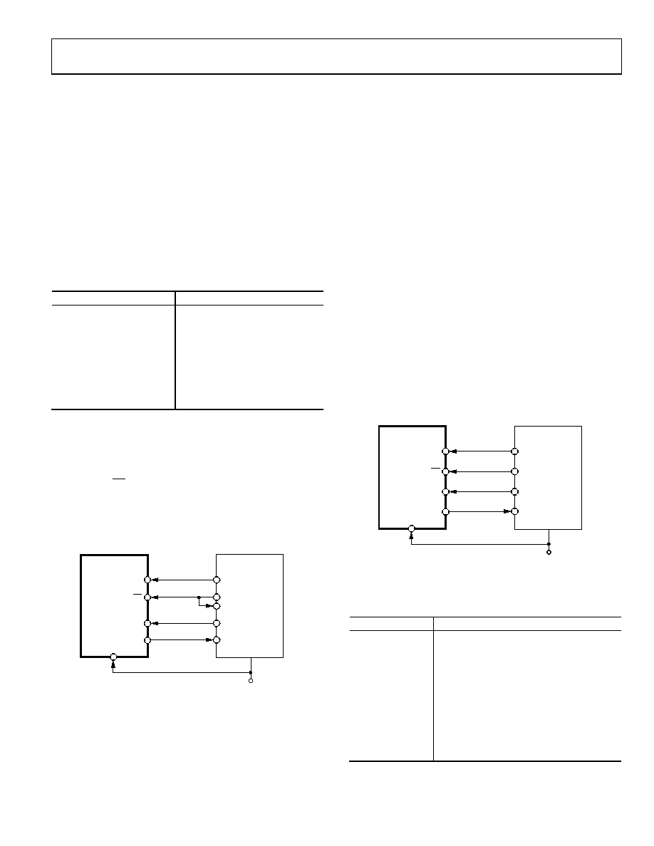
The connection diagram is shown in Figure 51. The ADSP-21xx
has TFS0 and RFS0 tied together. TFS0 is set as an output, and
RFS0 is set as an input. The DSP operates in alternative framing
mode, and the SPORT0 control register is set up as described in
Table 14. The frame synchronization signal generated on the
TFS is tied to CS and, as with all signal processing applications,
requires equidistant sampling. However, as in this example, the
timer interrupt is used to control the sampling rate of the ADC
and under certain conditions equidistant sampling cannot be
achieved.
AD73221
ADSP-21xx1
SCLK
SCLK0
CS
TFS0
RFS0
DOUT
DIN
DT0
DR0
VDD
VDRIVE
1ADDITIONAL PINS OMITTED FOR CLARITY.
04863-
037
Figure 51. Interfacing the AD7322 to the ADSP-21xx
The timer registers are loaded with a value that provides an
interrupt at the required sampling interval. When an interrupt
is received, a value is transmitted with TFS/DT (ADC control
word). The TFS is used to control the RFS and, therefore, the
reading of data.
The frequency of the serial clock is set in the SCLKDIV register.
When the instruction to transmit with TFS is given (AX0 = TX0),
the state of the serial clock is checked. The DSP waits until the
SCLK goes high, low, and then high again before starting the
transmission. If the timer and SCLK are chosen so that the
instruction to transmit occurs on or near the rising edge of
SCLK, data can be transmitted either immediately or at the next
clock edge.
For example, the ADSP-2111 has a master clock frequency of
16 MHz. If the SCLKDIV register is loaded with the value 3,
an SCLK of 2 MHz is obtained, and eight master clock periods
elapse for every one SCLK period. If the timer registers are loaded
with the value 803, 100.5 SCLKs occur between interrupts and,
subsequently, between transmit instructions. This situation leads
to nonequidistant sampling because the transmit instruction occurs
on an SCLK edge. If the number of SCLKs between interrupts is
an integer of N, equidistant sampling is implemented by the DSP.
The ADSP-BF53x family of DSPs interface directly to the
AD7322 without requiring glue logic, as shown in Figure 52.
The SPORT0 Receive Configuration 1 register should be set up
as outlined in Table 15.
AD73221
ADSP-BF53x1
VDD
VDRIVE
SCLK
RSCLK0
DIN
DT0
DOUT
DR0
CS
RFS0
1ADDITIONAL PINS OMITTED FOR CLARITY.
04863-
038
Figure 52. Interfacing the AD7322 to the ADSP-BF53x
Table 15. SPORT0 Receive Configuration 1 Register
Setting
Description
RCKFE = 1
Sample data with falling edge of RSCLK
LRFS = 1
Active low frame signal
RFSR = 1
Frame every word
IRFS = 1
Internal RFS used
RLSBIT = 0
Receive MSB first
RDTYPE = 00
Zero fill
IRCLK = 1
Internal receive clock
RSPEN = 1
Receive enable
SLEN = 1111
16-bit data-word
TFSR = RFSR = 1
Transmit and receive frame sync
相关PDF资料 |
PDF描述 |
|---|---|
| EEM31DTMS | CONN EDGECARD 62POS R/A .156 SLD |
| 0210490887 | CABLE JUMPER 1.25MM .152M 19POS |
| GEM30DRMI | CONN EDGECARD 60POS .156 SQ WW |
| EEM28DTKH | CONN EDGECARD 56POS DIP .156 SLD |
| EVAL-AD7484CBZ | BOARD EVALUATION FOR AD7484 |
相关代理商/技术参数 |
参数描述 |
|---|---|
| EVAL-AD7323CB | 制造商:AD 制造商全称:Analog Devices 功能描述:500 kSPS, 4-Channel, Software-Selectable, True Bipolar Input, 12-Bit Plus Sign ADC |
| EVAL-AD7323CBZ | 功能描述:BOARD EVALUATION FOR AD7323CBZ RoHS:是 类别:编程器,开发系统 >> 评估板 - 模数转换器 (ADC) 系列:iCMOS® 产品培训模块:Obsolescence Mitigation Program 标准包装:1 系列:- ADC 的数量:1 位数:12 采样率(每秒):94.4k 数据接口:USB 输入范围:±VREF/2 在以下条件下的电源(标准):- 工作温度:-40°C ~ 85°C 已用 IC / 零件:MAX11645 已供物品:板,软件 |
| EVAL-AD7324CB | 制造商:AD 制造商全称:Analog Devices 功能描述:4-Channel, Software-Selectable, True Bipolar Input, 12-Bit Plus Sign ADC |
| EVAL-AD7324CBZ | 功能描述:BOARD EVALUATION FOR AD7324CBZ RoHS:是 类别:编程器,开发系统 >> 评估板 - 模数转换器 (ADC) 系列:iCMOS® 产品培训模块:Obsolescence Mitigation Program 标准包装:1 系列:- ADC 的数量:1 位数:12 采样率(每秒):94.4k 数据接口:USB 输入范围:±VREF/2 在以下条件下的电源(标准):- 工作温度:-40°C ~ 85°C 已用 IC / 零件:MAX11645 已供物品:板,软件 |
| EVAL-AD7327CB | 制造商:AD 制造商全称:Analog Devices 功能描述:500 kSPS, 8-Channel, Software-Selectable, True Bipolar Input, 12-Bit Plus Sign ADC |
发布紧急采购,3分钟左右您将得到回复。