- 您现在的位置:买卖IC网 > PDF目录17050 > EVAL-AD7763EDZ (Analog Devices Inc)BOARD EVAL CONTROL AD7763 PDF资料下载
参数资料
| 型号: | EVAL-AD7763EDZ |
| 厂商: | Analog Devices Inc |
| 文件页数: | 11/33页 |
| 文件大小: | 0K |
| 描述: | BOARD EVAL CONTROL AD7763 |
| 标准包装: | 1 |
| ADC 的数量: | 1 |
| 位数: | 24 |
| 采样率(每秒): | 625k |
| 数据接口: | 并联 |
| 输入范围: | ±3.25 Vpp |
| 在以下条件下的电源(标准): | 955.5mW @ 625kSPS |
| 工作温度: | -40°C ~ 85°C |
| 已用 IC / 零件: | AD7763 |
| 已供物品: | 板,CD |
第1页第2页第3页第4页第5页第6页第7页第8页第9页第10页当前第11页第12页第13页第14页第15页第16页第17页第18页第19页第20页第21页第22页第23页第24页第25页第26页第27页第28页第29页第30页第31页第32页第33页
AD7763
Data Sheet
Rev. B | Page 18 of 32
READING DATA USING THE I2S INTERFACE
interface. The interface is functional only for the output of
stereo data and does not apply to writing to control registers,
programming coefficients for the digital filter, or the reading of
any information contained in the AD7763 onboard registers.
All of these operations must be undertaken using the normal
serial interface.
shown in Table 9 are used as the output pins for the SCK (serial
clock), SD (serial data), and WS (word select) signals for the I2S
interface.
Table 9.
SPI Pins
I2S Signals
FSO
WS
SDO
SD
SCO
SCK
To enable the I2S interface, the I2S pin is set to logic high. The
interface are set to 001. The Address Pins ADR[2:0] of the two
devices must also be set to 000 and 001, respectively.
The WS and SCK signals that are used for the interface can be
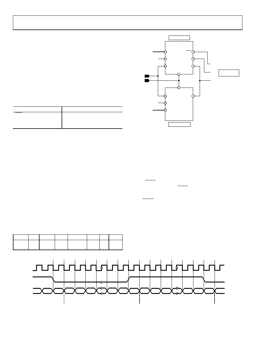
taken from either AD7763 device. Note that the device that is
assigned Address 000 is defined as the left channel, and its data
is output on the SD line when WS is logic low.
The WS and SCK signals can be taken from the appropriate
The SD pins of both devices must be connected together, as
shown in Figure 27.
Data is clocked out on the SD line in accordance with Figure 28.
Because Device A is assigned Address 000, it is defined as the
left channel. The 32-bit conversion result from the left channel
is clocked out when WS is logic low, with the MSB being clocked
out first. Each 32-bit result consists of 24 data bits in twos
complement format, followed by eight status bits, as shown in
the following bit map.
D7
D6
D5
D4
D3
D2
D1
D0
DVALID
OVR
UFILTER
LPWR FILTER_OK
ADR0
0
Three-
State
AD7763
(000)
MCLK
LEFT CHANNEL
RIGHT CHANNEL
DEVICE
ADDRESS
000
DEVICE
ADDRESS
001
1
001
ADR[2:0]
FSO
WS
A
SH[2:0]
I2S
SH[2:0]
MCLK
SCO
SDO
SD
SCK
3-WIRE
I2S INTERFACE
05476-
026
AD7763
(001)
MCLK
1
SH[2:0]
SDO
B
ADR[2:0]
I2S
Conversion results from Device B, assigned Address 001, are
clocked out on the SD line when WS is logic high. The SD line
goes into three-state on the falling edge of the 32nd SCK after
the falling edge of WS (left channel data) and also on the falling
edge of the 32nd SCK after the rising edge of WS (right channel
data). This permits swapping of the SD bus between the left and
right channel devices without contention.
In decimate × 32 mode the I2S interface is operational only
when CDIV = 0 and SCR = 1. The interface operates for all
combinations of SCR and CDIV in all other modes of
decimation.
The DRDY pulse still operates as in the normal serial SPI-type
interface, pulsing low immediately prior to the falling edge of
WS but having no meaning in the I2S interface specification.
ST1
ST2
D21
THREE-
STATE
D22
THREE-
STATE
THREE-
STATE
D23
D21
D22
RIGHT CHANNEL
DEVICE B
(WORD n – 1)
RIGHT CHANNEL
DEVICE B
(WORD n + 1)
LEFT CHANNEL
DEVICE A
(WORD n + 2)
LEFT CHANNEL
DEVICE A
(WORD n)
D23
SCK A (O)
WS A (O)
SD (O)
ST1
ST2
05476-
027
Figure 28. Timing Diagram for I2S Interface
相关PDF资料 |
PDF描述 |
|---|---|
| EVAL-AD7401AEDZ | BOARD EVAL FOR AD7401 |
| HI5860SOICEVAL1 | EVALUATION PLATFORM SOIC HI5860 |
| REC5-0505DRW/H2/A | CONV DC/DC 5W 4.5-9VIN +/-05VOUT |
| REC5-483.3DRW/H2/C | CONV DC/DC 5W 36-72VIN +/-3.3V |
| GCM22DCMH | CONN EDGECARD 44POS .156 WW |
相关代理商/技术参数 |
参数描述 |
|---|---|
| EVAL-AD7764EBZ | 制造商:Analog Devices 功能描述:EVAL BD FOR AD7764 - Bulk |
| EVAL-AD7764EDZ | 功能描述:BOARD EVAL AD7764 RoHS:是 类别:编程器,开发系统 >> 评估板 - 模数转换器 (ADC) 系列:- 产品培训模块:Obsolescence Mitigation Program 标准包装:1 系列:- ADC 的数量:1 位数:12 采样率(每秒):94.4k 数据接口:USB 输入范围:±VREF/2 在以下条件下的电源(标准):- 工作温度:-40°C ~ 85°C 已用 IC / 零件:MAX11645 已供物品:板,软件 |
| EVAL-AD7765EBZ | 制造商:Analog Devices 功能描述:EVAL BOARD 24BIT, 312KSPS, 109DB - Bulk |
| EVAL-AD7765EDZ | 功能描述:BOARD EVAL AD7765 RoHS:是 类别:编程器,开发系统 >> 评估板 - 模数转换器 (ADC) 系列:- 产品培训模块:Obsolescence Mitigation Program 标准包装:1 系列:- ADC 的数量:1 位数:12 采样率(每秒):94.4k 数据接口:USB 输入范围:±VREF/2 在以下条件下的电源(标准):- 工作温度:-40°C ~ 85°C 已用 IC / 零件:MAX11645 已供物品:板,软件 |
| EVAL-AD7766-1EDZ | 功能描述:BOARD EVAL AD7766-1 64KSPS 111DB RoHS:是 类别:编程器,开发系统 >> 评估板 - 模数转换器 (ADC) 系列:- 产品培训模块:Obsolescence Mitigation Program 标准包装:1 系列:- ADC 的数量:1 位数:12 采样率(每秒):94.4k 数据接口:USB 输入范围:±VREF/2 在以下条件下的电源(标准):- 工作温度:-40°C ~ 85°C 已用 IC / 零件:MAX11645 已供物品:板,软件 |
发布紧急采购,3分钟左右您将得到回复。