- 您现在的位置:买卖IC网 > PDF目录17050 > EVAL-AD7763EDZ (Analog Devices Inc)BOARD EVAL CONTROL AD7763 PDF资料下载
参数资料
| 型号: | EVAL-AD7763EDZ |
| 厂商: | Analog Devices Inc |
| 文件页数: | 7/33页 |
| 文件大小: | 0K |
| 描述: | BOARD EVAL CONTROL AD7763 |
| 标准包装: | 1 |
| ADC 的数量: | 1 |
| 位数: | 24 |
| 采样率(每秒): | 625k |
| 数据接口: | 并联 |
| 输入范围: | ±3.25 Vpp |
| 在以下条件下的电源(标准): | 955.5mW @ 625kSPS |
| 工作温度: | -40°C ~ 85°C |
| 已用 IC / 零件: | AD7763 |
| 已供物品: | 板,CD |
第1页第2页第3页第4页第5页第6页当前第7页第8页第9页第10页第11页第12页第13页第14页第15页第16页第17页第18页第19页第20页第21页第22页第23页第24页第25页第26页第27页第28页第29页第30页第31页第32页第33页
AD7763
Data Sheet
Rev. B | Page 14 of 32
THEORY OF OPERATION
The AD7763 employs a Σ-Δ conversion technique to convert
the analog input into an equivalent digital word. The modulator
samples the input waveform and outputs an equivalent digital
word to the digital filter at a rate equal to ICLK.
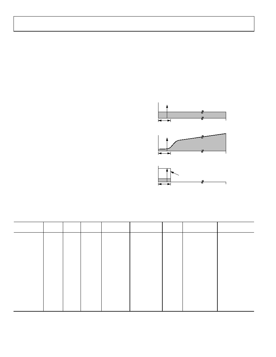
Due to the high oversampling rate, which spreads the quanti-
zation noise from 0 to f
ICLK, the noise energy contained in the
band of interest is reduced (see Figure 23). To further reduce
quantization noise, a high order modulator is employed to shape
the noise spectrum; thus, most of the noise energy is shifted
out of the band of interest (see Figure 24).
The digital filtering that follows the modulator removes the
large out-of-band quantization noise (see Figure 25), while
also reducing the data rate from f
ICLK at the input of the filter
to f
ICLK/32 or less at the output of the filter, depending on the
decimation rate used.
Digital filtering has certain advantages over analog filtering.
It does not introduce significant noise or distortion and can
be made perfectly linear phase.
The AD7763 employs three finite impulse response (FIR) filters
in series. By using different combinations of decimation ratios
and filter selection, data can be obtained from the AD7763 at
four different data rates. The first filter receives data from the
modulator at ICLK
MHz, where it is decimated × 4 to output
data at (ICLK/4)
MHz.
The second filter allows the decimation rate to be chosen from
8× to 32×. The third filter has a fixed decimation rate of 2×, is
user programmable, and has a default configuration (see the
Programmable FIR Filter section). This filter can be bypassed.
Table 6 shows some characteristics of the default filter. The group
delay of the filter is defined as the delay to the center of the
impulse response and is equal to the computation plus filter
delays. The delay until valid data is available (the DVALID status bit
is set) is equal to 2× the filter delay plus the computation delay.
05
47
6-
0
2
4
QUANTIZATION NOISE
fICLK/2
BAND OF INTEREST
Figure 23. Σ-Δ ADC, Quantization Noise
05
47
6-
02
5
fICLK/2
NOISE SHAPING
BAND OF INTEREST
Figure 24. Σ-Δ ADC, Noise Shaping
05
47
6-
01
2
fICLK/2
BAND OF INTEREST
DIGITAL FILTER CUTOFF FREQUENCY
Figure 25. Σ-Δ ADC, Digital Filter Cutoff Frequency
Table 6. Configuration With Default Filter
ICLK
Frequency
Filter 1
Filter 2
Filter 3
Data State
Computation
Delay
Filter
Delay
Pass Band
Bandwidth
Output Data Rate
(ODR)
20 MHz
4×
2×
Fully filtered
1.775 μs
44.4 μs
250 kHz
625 kHz
20 MHz
4×
8×
Bypassed
Partially
filtered
2.6 μs
10.8 μs
140.625 kHz
625 kHz
20 MHz
4×
8×
2×
Fully filtered
2.25 μs
87.6 μs
125 kHz
312.5 kHz
20 MHz
4×
16×
Bypassed
Partially
filtered
4.175 μs
20.4 μs
70.3125 kHz
312.5 kHz
20 MHz
4×
16×
2×
Fully filtered
3.1 μs
174 μs
62.5 kHz
156.25 kHz
20 MHz
4×
32×
Bypassed
Partially
filtered
7.325 μs
39.6 μs
35.156 kHz
156.25 kHz
20 MHz
4×
32×
2×
Fully filtered
4.65 μs
346.8 μs
31.25 kHz
78.125 kHz
12.288 MHz
4×
8×
2×
Fully filtered
3.66 μs
142.6 μs
76.8 kHz
192 kHz
12.288 MHz
4×
16×
2×
Fully filtered
5.05 μs
283.2 μs
38.4 kHz
96 kHz
12.288 MHz
4×
32×
Bypassed
Partially
filtered
11.92 μs
64.45 μs
21.6 kHz
96 kHz
12.288 MHz
4×
32×
2×
Fully filtered
7.57 μs
564.5 μs
19.2 kHz
48 kHz
相关PDF资料 |
PDF描述 |
|---|---|
| EVAL-AD7401AEDZ | BOARD EVAL FOR AD7401 |
| HI5860SOICEVAL1 | EVALUATION PLATFORM SOIC HI5860 |
| REC5-0505DRW/H2/A | CONV DC/DC 5W 4.5-9VIN +/-05VOUT |
| REC5-483.3DRW/H2/C | CONV DC/DC 5W 36-72VIN +/-3.3V |
| GCM22DCMH | CONN EDGECARD 44POS .156 WW |
相关代理商/技术参数 |
参数描述 |
|---|---|
| EVAL-AD7764EBZ | 制造商:Analog Devices 功能描述:EVAL BD FOR AD7764 - Bulk |
| EVAL-AD7764EDZ | 功能描述:BOARD EVAL AD7764 RoHS:是 类别:编程器,开发系统 >> 评估板 - 模数转换器 (ADC) 系列:- 产品培训模块:Obsolescence Mitigation Program 标准包装:1 系列:- ADC 的数量:1 位数:12 采样率(每秒):94.4k 数据接口:USB 输入范围:±VREF/2 在以下条件下的电源(标准):- 工作温度:-40°C ~ 85°C 已用 IC / 零件:MAX11645 已供物品:板,软件 |
| EVAL-AD7765EBZ | 制造商:Analog Devices 功能描述:EVAL BOARD 24BIT, 312KSPS, 109DB - Bulk |
| EVAL-AD7765EDZ | 功能描述:BOARD EVAL AD7765 RoHS:是 类别:编程器,开发系统 >> 评估板 - 模数转换器 (ADC) 系列:- 产品培训模块:Obsolescence Mitigation Program 标准包装:1 系列:- ADC 的数量:1 位数:12 采样率(每秒):94.4k 数据接口:USB 输入范围:±VREF/2 在以下条件下的电源(标准):- 工作温度:-40°C ~ 85°C 已用 IC / 零件:MAX11645 已供物品:板,软件 |
| EVAL-AD7766-1EDZ | 功能描述:BOARD EVAL AD7766-1 64KSPS 111DB RoHS:是 类别:编程器,开发系统 >> 评估板 - 模数转换器 (ADC) 系列:- 产品培训模块:Obsolescence Mitigation Program 标准包装:1 系列:- ADC 的数量:1 位数:12 采样率(每秒):94.4k 数据接口:USB 输入范围:±VREF/2 在以下条件下的电源(标准):- 工作温度:-40°C ~ 85°C 已用 IC / 零件:MAX11645 已供物品:板,软件 |
发布紧急采购,3分钟左右您将得到回复。