- 您现在的位置:买卖IC网 > PDF目录17050 > EVAL-AD7763EDZ (Analog Devices Inc)BOARD EVAL CONTROL AD7763 PDF资料下载
参数资料
| 型号: | EVAL-AD7763EDZ |
| 厂商: | Analog Devices Inc |
| 文件页数: | 2/33页 |
| 文件大小: | 0K |
| 描述: | BOARD EVAL CONTROL AD7763 |
| 标准包装: | 1 |
| ADC 的数量: | 1 |
| 位数: | 24 |
| 采样率(每秒): | 625k |
| 数据接口: | 并联 |
| 输入范围: | ±3.25 Vpp |
| 在以下条件下的电源(标准): | 955.5mW @ 625kSPS |
| 工作温度: | -40°C ~ 85°C |
| 已用 IC / 零件: | AD7763 |
| 已供物品: | 板,CD |
第1页当前第2页第3页第4页第5页第6页第7页第8页第9页第10页第11页第12页第13页第14页第15页第16页第17页第18页第19页第20页第21页第22页第23页第24页第25页第26页第27页第28页第29页第30页第31页第32页第33页
Data Sheet
AD7763
Rev. B | Page 9 of 32
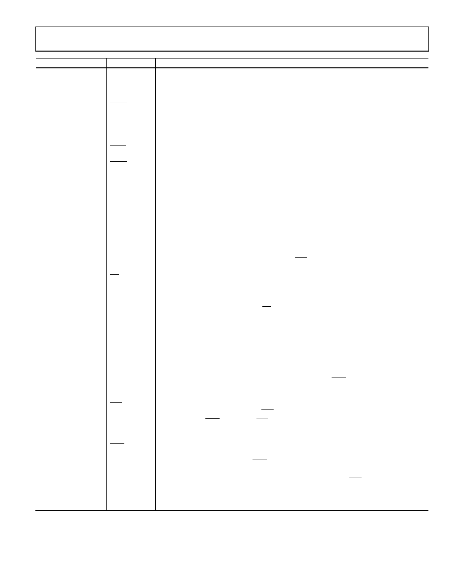
Pin No.
Mnemonic
Description
8
DECAPA
Decoupling Pin. A 100 nF capacitor must be inserted between this pin and AGND1.
30
DECAPB
Decoupling Pin. A 33 pF capacitor must be inserted between this pin and AGND3.
17
RBIAS
Bias Current Setting. A resistor must be inserted between this pin and AGND.
See the Bias Resistor Selection section.
37
RESET
A falling edge on this pin resets all internal digital circuitry. Holding this pin low
keeps the AD7763 in a reset state.
3
MCLK
Master Clock Input. A low jitter digital clock must be applied to this pin. The output data rate
depends on the frequency of this clock. See the Clocking the AD7763 section.
2
MCLKGND
Master Clock Ground Sensing Pin.
36
SYNC
Synchronization Input. A falling edge on this pin resets the internal filter. This can be used
to synchronize multiple devices in a system.
38
DRDY
Data Ready Output. Each time new conversion data is available, an active low pulse,
ICLK period wide, is produced on this pin. See the AD7763 Interface section.
39, 40, 45
SH2:0
Share Pins 2:0. For multiple AD7763 devices sharing a common serial bus. Each device is wired
with the binary value that represents the number of devices sharing the serial bus. SH2 is the
MSB. See the Sharing the Serial Bus section.
46 to 48
ADR2:0
Address 2:0. Allows multiple AD7763 devices to share a common serial bus. Each device must be
programmed with an individual address using these three pins. See the Sharing the Serial Bus
section.
49
SCP
Serial Clock Polarity. Determines on which edge of SCO the data bits are clocked out and on
which edge they are valid. All timing diagrams are shown with SCP = 0, and all SCO edges
shown should be inverted for SCP = 1.
50
SDL
Serial Data Latch. A pulse is output on this pin after every 16 data bits. The pulse is one SCO
period wide and can be used in conjunction with FSO as an alternative framing method for
serial transfers requiring a framing signal more frequent than every 32 bits.
51
FSI
Frame Sync In. The status of this pin is checked on the falling edge of SCO. If this pin is low, then
the first data bit is latched in on the next SCO falling edge when SCP = 0 or on the rising edge of
SCO if SCP = 1.
52
SDI
Serial Data In. The first data bit (MSB) must be valid on the next SCO falling edge when SCP = 0
(or SCO rising edge SCP = 1) after the FSI event has been latched. Each write requires 32 bits: the
ALL bit, 3 address bits, and 12 register address bits, followed by the remaining 16 bits of data to
be written to the device.
54
SDO
Serial Data Out. Address, status, and data bits are clocked out on this line during each serial
transfer.
If SCP = 0, each bit is clocked out on an SCO rising edge and is valid on the falling edge. When
the I2S pin is set to logic high, this pin outputs the signal defined as SD in the I2S bus
specification. See the Reading Data Using the I2S Interface section for details.
55
SCO
Serial Clock Out. This clock signal is derived from the internal ICLK signal. The frequency of SCO
is equal to either ICLK or ICLK/2, depending on the state of the CDIV and SCR pins (see the
56
FSO
Frame Sync Out. This signal frames the serial data output and is 32 SCO periods wide. The
exception to the framing behavior of FSO occurs in decimate × 32 mode, where, for certain
combinations of CDIV and SCR, the FSO signal is constantly logic low. See the Reading Data
58
CDIV
Clock Divider. This pin is used to select the ratio of MCLK to ICLK. See the AD7763 Interface
section.
60
SCR
Serial Clock Rate. This pin and the CDIV pin program the SCO frequency (see Table 7).
61
I2S
I2S Select. A Logic 1 on this pin changes the serial data-out mode from SPI to I2S. The SDO pin
outputs as the SD signal, the SCO pin outputs the SCK signal, and the FSO pin outputs the WS
See the Reading Data Using the I2S Interface section for further details.
EPAD
Exposed Pad. Connect the exposed pad to AGNDx with six to eight vias.
相关PDF资料 |
PDF描述 |
|---|---|
| EVAL-AD7401AEDZ | BOARD EVAL FOR AD7401 |
| HI5860SOICEVAL1 | EVALUATION PLATFORM SOIC HI5860 |
| REC5-0505DRW/H2/A | CONV DC/DC 5W 4.5-9VIN +/-05VOUT |
| REC5-483.3DRW/H2/C | CONV DC/DC 5W 36-72VIN +/-3.3V |
| GCM22DCMH | CONN EDGECARD 44POS .156 WW |
相关代理商/技术参数 |
参数描述 |
|---|---|
| EVAL-AD7764EBZ | 制造商:Analog Devices 功能描述:EVAL BD FOR AD7764 - Bulk |
| EVAL-AD7764EDZ | 功能描述:BOARD EVAL AD7764 RoHS:是 类别:编程器,开发系统 >> 评估板 - 模数转换器 (ADC) 系列:- 产品培训模块:Obsolescence Mitigation Program 标准包装:1 系列:- ADC 的数量:1 位数:12 采样率(每秒):94.4k 数据接口:USB 输入范围:±VREF/2 在以下条件下的电源(标准):- 工作温度:-40°C ~ 85°C 已用 IC / 零件:MAX11645 已供物品:板,软件 |
| EVAL-AD7765EBZ | 制造商:Analog Devices 功能描述:EVAL BOARD 24BIT, 312KSPS, 109DB - Bulk |
| EVAL-AD7765EDZ | 功能描述:BOARD EVAL AD7765 RoHS:是 类别:编程器,开发系统 >> 评估板 - 模数转换器 (ADC) 系列:- 产品培训模块:Obsolescence Mitigation Program 标准包装:1 系列:- ADC 的数量:1 位数:12 采样率(每秒):94.4k 数据接口:USB 输入范围:±VREF/2 在以下条件下的电源(标准):- 工作温度:-40°C ~ 85°C 已用 IC / 零件:MAX11645 已供物品:板,软件 |
| EVAL-AD7766-1EDZ | 功能描述:BOARD EVAL AD7766-1 64KSPS 111DB RoHS:是 类别:编程器,开发系统 >> 评估板 - 模数转换器 (ADC) 系列:- 产品培训模块:Obsolescence Mitigation Program 标准包装:1 系列:- ADC 的数量:1 位数:12 采样率(每秒):94.4k 数据接口:USB 输入范围:±VREF/2 在以下条件下的电源(标准):- 工作温度:-40°C ~ 85°C 已用 IC / 零件:MAX11645 已供物品:板,软件 |
发布紧急采购,3分钟左右您将得到回复。