- 您现在的位置:买卖IC网 > PDF目录67412 > FAN5019MTCX_NL (FAIRCHILD SEMICONDUCTOR CORP) SWITCHING CONTROLLER, 4000 kHz SWITCHING FREQ-MAX, PDSO28 PDF资料下载
参数资料
| 型号: | FAN5019MTCX_NL |
| 厂商: | FAIRCHILD SEMICONDUCTOR CORP |
| 元件分类: | 稳压器 |
| 英文描述: | SWITCHING CONTROLLER, 4000 kHz SWITCHING FREQ-MAX, PDSO28 |
| 封装: | LEAD FREE, TSSOP-28 |
| 文件页数: | 12/30页 |
| 文件大小: | 781K |
| 代理商: | FAN5019MTCX_NL |
第1页第2页第3页第4页第5页第6页第7页第8页第9页第10页第11页当前第12页第13页第14页第15页第16页第17页第18页第19页第20页第21页第22页第23页第24页第25页第26页第27页第28页第29页第30页
FAN5019
PRODUCT SPECIFICATION
2
REV. 1.0.7 1/5/04
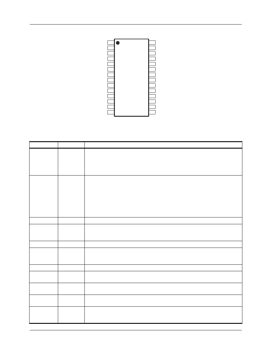
Pin Assignments
Pin Denitions
Pin Number
Pin Name
Pin Function Description
1–5
VID [4:0]
VID inputs. Determines the output voltage via the internal DAC. These inputs
comply to VRM10/VRD10 specifications for static and dynamic operation. All have
internal pull-ups (1.25V for VRM10 and 2.5V for VRM9) so leaving them open
results in logic high. Leaving VID[4:0] open results in a "No CPU" condition
disabling the PWM outputs.
6
VID5/SEL
VID5 Input/DAC Select. Dual function pin that is either the 12.5mV DAC LSB for
VRM10 or selects the VRM9 DAC codes when forced higher than Vtblsel(VRM9)
voltage. The truth table is as follows:
VVID5/SEL held > Vtblsel(VRM9); VRM9 DAC table is selected (See Table 3)
VViD5/SEL < Vtblsel(VRM10); VRM10 DAC table is selected (See Table 2) and
VViD5/SEL pin is used as VID5 input.
7
FBRTN
Feedback Return. Error Amp and DAC reference point.
8FB
Feedback Input. Inverting input for Error Amp this pin is used for external
compensation. This pin can also be used to introduce DC offset voltage to the
output.
9
COMP
Error Amp output. This pin is used for external compensation.
10
PWRGD
Power Good output. This is an open-drain output that asserts when the output
voltage is within the specified tolerance. It is expected to be pulled up to an external
voltage rail.
11
EN
Enable. Logic signal that enables the controller when logic high.
12
DELAY
Soft-start and Current Limit Delay. An external resistor and capacitor sets the
softstart ramp rate and the over-current latch off delay.
13
RT
Switching Frequency Adjust. This pin adjusts the output PWM switching
frequency via an external resistor.
14
RAMPADJ
PWM Current Ramp Adjust. An external resistor to Vcc will adjust the amplitude of
the internal PWM ramp.
15
ILIMIT
Current Limit Adjust. An external resistor sets the current limit threshold for the
regulator circuit. This pin is internally pulled low when EN is low or the UVLO circuit
is active. It is also used to enable the drivers.
DELAY
VID4
VID3
VID2
VID1
VID0
COMP
CSCOMP
PWRGD
EN
CSSUM
RT
VCC
SW2
SW3
PWM3
PWM4
PWM1
GND
FBRTN
ILIMIT
FB
CSREF
RAMPADJ
1
2
3
4
5
6
7
8
9
10
11
12
13
14
28
27
26
25
24
23
22
21
20
19
18
17
16
15
FAN5019
TSSOP-28
SW1
PWM2
SW4
VID5/SEL
相关PDF资料 |
PDF描述 |
|---|---|
| FAN5037MX_NL | SWITCHING CONTROLLER, PDSO8 |
| FAN5037M_NL | SWITCHING CONTROLLER, PDSO8 |
| FAN5061M | SWITCHING CONTROLLER, 345 kHz SWITCHING FREQ-MAX, PDSO20 |
| FAN5201MSA | 6 A BATTERY CHARGE CONTROLLER, 275 kHz SWITCHING FREQ-MAX, PDSO24 |
| FAN5361UMP10X | SWITCHING REGULATOR, DSO6 |
相关代理商/技术参数 |
参数描述 |
|---|---|
| FAN501MPX | 制造商:Fairchild Semiconductor Corporation 功能描述:PWM CONTROLLER - Tape and Reel |
| FAN5020_AAC3116B WAF | 制造商:Fairchild Semiconductor Corporation 功能描述: |
| FAN5021_AAC3026B WAF | 制造商:Fairchild Semiconductor Corporation 功能描述: |
| FAN5026 | 制造商:FAIRCHILD 制造商全称:Fairchild Semiconductor 功能描述:Dual DDR/Dual-output PWM Controller |
| FAN5026_11 | 制造商:FAIRCHILD 制造商全称:Fairchild Semiconductor 功能描述:Dual DDR / Dual-Output PWM Controller |
发布紧急采购,3分钟左右您将得到回复。