- 您现在的位置:买卖IC网 > PDF目录370153 > FBGA FBGA - FBGA User's Guide. Version 4.2 PDF资料下载
参数资料
| 型号: | FBGA |
| 英文描述: | FBGA - FBGA User's Guide. Version 4.2 |
| 中文描述: | FBGA封装- FBGA封装用户指南。版本4.2 |
| 文件页数: | 54/97页 |
| 文件大小: | 2624K |
| 代理商: | FBGA |
第1页第2页第3页第4页第5页第6页第7页第8页第9页第10页第11页第12页第13页第14页第15页第16页第17页第18页第19页第20页第21页第22页第23页第24页第25页第26页第27页第28页第29页第30页第31页第32页第33页第34页第35页第36页第37页第38页第39页第40页第41页第42页第43页第44页第45页第46页第47页第48页第49页第50页第51页第52页第53页当前第54页第55页第56页第57页第58页第59页第60页第61页第62页第63页第64页第65页第66页第67页第68页第69页第70页第71页第72页第73页第74页第75页第76页第77页第78页第79页第80页第81页第82页第83页第84页第85页第86页第87页第88页第89页第90页第91页第92页第93页第94页第95页第96页第97页
FBGA User’s Guide
Version 4.2, November 1, 2002
53
Chapter 7:
Board Design and Layout Considerations
General Design Considerations
One of the first decisions to be made when designing boards for chip scale packages is whether it will
be possible to use conventional PCB technology and design rules, or whether microvia technology will
be necessary. Recently, microvia HDI (High Density Interconnects) boards have been adopted in
several volume applications, particularly in cell-phones and camcorders, and the prices of microvia
boards have been falling quickly. HDI are defined as having vias with a diameter less than 0.006 inch
on pad size of 0.014 inch or smaller. However they are still more expensive. Measured on the basis of
price per unit area per metal layer, microvia boards are at least twice as expensive as high-density
conventional multilayer PCBs, even with blind and buried vias. Furthermore, there is also the question
of availability: it may not be easy to find suppliers with production capacity for microvia boards.
It is for this reason that a pitch of 0.8 mm has been chosen for AMD’s FBGA. As shown in the next
section, single-layer routing for Flash Memory FBGA can be accomplished with line and space widths
of 0.005 inch or more. Because of the relatively low lead count, this can be done in one layer, but if
desired, connections down to inner layers can be accomplished through interstitial vias.
Solder-Mask Defined Versus Non-Solder-Mask Defined
There has been much discussion about the relative merits of solder-mask defined (SMD) and non-
solder-mask defined (NSMD) lands for attaching area array packages such as conventional BGA and
fine pitch BGA. AMD’s FBGA can be used with either, but there are two important benefits of NSMD
pads. One is that smaller copper pads can be used, thus providing more generous clearance for the
routing channels. (Another is that the solder can wet around the sides of the pad during reflow (see
Figure 7-1) thus providing a stronger joint.)
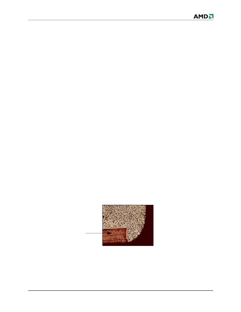
Figure 7-1. Solder Wetting Around Pad During Reflow
Note that if the kind of wetting shown in Figure 7-1 is desired, it is important to provide sufficient
clearance of solder mask around the pad. The PCB supplier may consider the edge of the solder mask
touching the edge of the pad to be acceptable, however, this condition would prevent the solder from
completely wetting the side of the pad.
Copper attachment pad
相关PDF资料 |
PDF描述 |
|---|---|
| FBI1.5A4S1 | Bridge Rectifiers (In Line) |
| FBI1.5B4S1 | Bridge Rectifiers (In Line) |
| FBI1.5B5S2 | Bridge Rectifiers (In Line) |
| FBI1.5D4S1 | Bridge Rectifiers (In Line) |
| FBI1.5D5S2 | Bridge Rectifiers (In Line) |
相关代理商/技术参数 |
参数描述 |
|---|---|
| FBGA96T.5-DC144 | 制造商:未知厂家 制造商全称:未知厂家 功能描述:FBGA96T.5-DC144 |
| FBGA-SD | 制造商:STATSCHIP 制造商全称:STATSCHIP 功能描述:Fine Pitch Ball Grid Array - Stacked Die |
| FBGC-1.44G | 制造商:MERRIMAC 制造商全称:MERRIMAC 功能描述:FILTER |
| FBGC-2.75G | 制造商:MERRIMAC 制造商全称:MERRIMAC 功能描述:FILTER |
| FBGC-3-1.4G | 制造商:MERRIMAC 制造商全称:MERRIMAC 功能描述:FILTER |
发布紧急采购,3分钟左右您将得到回复。