- 您现在的位置:买卖IC网 > Datasheet目录415 > FDC6303N (Fairchild Semiconductor)IC FET DGTL N-CH DUAL 25V SSOT6 Datasheet资料下载
参数资料
| 型号: | FDC6303N |
| 厂商: | Fairchild Semiconductor |
| 文件页数: | 1/5页 |
| 文件大小: | 0K |
| 描述: | IC FET DGTL N-CH DUAL 25V SSOT6 |
| 产品培训模块: | High Voltage Switches for Power Processing |
| 产品变化通告: | Design/Process Change 11/May/2007 Mold Compound Change 08/April/2008 |
| 标准包装: | 1 |
| FET 型: | 2 个 N 沟道(双) |
| FET 特点: | 逻辑电平门 |
| 漏极至源极电压(Vdss): | 25V |
| 电流 - 连续漏极(Id) @ 25° C: | 680mA |
| 开态Rds(最大)@ Id, Vgs @ 25° C: | 450 毫欧 @ 500mA,4.5V |
| Id 时的 Vgs(th)(最大): | 1.5V @ 250µA |
| 闸电荷(Qg) @ Vgs: | 2.3nC @ 4.5V |
| 输入电容 (Ciss) @ Vds: | 50pF @ 10V |
| 功率 - 最大: | 700mW |
| 安装类型: | 表面贴装 |
| 封装/外壳: | SOT-23-6 细型,TSOT-23-6 |
| 供应商设备封装: | 6-SSOT |
| 包装: | 标准包装 |
| 产品目录页面: | 1216 (CN2011-ZH PDF) |
| 其它名称: | FDC6303NDKR |
�� �
�
�August� 1997�
�FDC6303N�
�Digital� FET,� Dual� N-Channel�
�General� Description�
�These� dual� N-Channel� logic� level� enhancement� mode� field�
�effect� transistors� are� produced� using� Fairchild's� proprietary,�
�high� cell� density,� DMOS� technology.� This� very� high� density�
�process� is� especially� tailored� to� minimize� on-state�
�resistance.� This� device� has� been� designed� especially� for�
�low� voltage� applications� as� a� replacement� for� digital�
�transistors� in� load� switching� applications.� Since� bias�
�resistors� are� not� required� this� one� N-Channel� FET� can�
�replace� several� digital� transistors� with� different� bias�
�resistors� like� the� IMHxA� series.�
�Features�
�25� V,� 0.68� A� continuous,� 2� A� Peak.�
�R� DS(ON)� =� 0.6� ?� @� V� GS� =� 2.7� V�
�R� DS(ON)� =� 0.45� ?� @� V� GS� =� 4.5� V.�
�Very� low� level� gate� drive� requirements� allowing� direct�
�operation� in� 3V� circuits.� V� GS(th)� <� 1.5� V.�
�Gate-Source� Zener� for� ESD� ruggedness.�
�>6kV� Human� Body� Model�
�Replace� multiple� NPN� digital� transistors� (IMHxA� series)�
�with� one� DMOS� FET.�
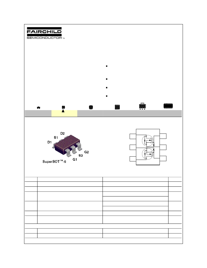
�SOT-23�
�SuperSOT� TM� -6�
�SuperSOT� TM� -8�
�SO-8�
�SOT-223�
�SOIC-16�
�Mark:� .303�
�4�
�5�
�6�
�3�
�2�
�1�
�Absolute� Maximum� Ratings�
�T� A� =� 25°C� unless� otherwise� noted�
�Symbol�
�V� DSS�
�V� GSS�
�Parameter�
�Drain-Source� Voltage�
�Gate-Source� Voltage�
�FDC6303N�
�25�
�8�
�Units�
�V�
�V�
�I� D�
�Drain� Current�
�-� Continuous�
�0.68�
�A�
�-� Pulsed�
�2�
�P� D�
�Maximum� Power� Dissipation�
�(Note� 1a)�
�0.9�
�W�
�(Note� 1b)�
�0.7�
�T� J� ,T� STG�
�ESD�
�Operating� and� Storage� Temperature� Range�
�Electrostatic� Discharge� Rating� MIL-STD-883D�
�-55� to� 150�
�6.0�
�°C�
�kV�
�Human� Body� Model� (100pf� /� 1500� Ohm)�
�THERMAL� CHARACTERISTICS�
�R� θ� JA�
�R� θ� JC�
�Thermal� Resistance,� Junction-to-Ambient�
�Thermal� Resistance,� Junction-to-Case�
�(Note� 1a)�
�(Note� 1)�
�140�
�60�
�°C/W�
�°C/W�
�?� 1997� Fairchild� Semiconductor� Corporation�
�FDC6303N� Rev.C�
�相关PDF资料 |
PDF描述 |
|---|---|
| FDC6304P | MOSFET P-CH DUAL 25V SSOT-6 |
| FDC6305N | MOSFET N-CHAN DUAL 20V SSOT6 |
| FDC6306P | MOSFET P-CHAN DUAL 20V SSOT6 |
| FDC6310P | MOSFET P-CH DUAL 20V SSOT-6 |
| FDC6312P | MOSFET P-CH DUAL 20V SSOT-6 |
相关代理商/技术参数 |
参数描述 |
|---|---|
| FDC6303N_Q | 功能描述:MOSFET SSOT-6 N-CH 25V RoHS:否 制造商:STMicroelectronics 晶体管极性:N-Channel 汲极/源极击穿电压:650 V 闸/源击穿电压:25 V 漏极连续电流:130 A 电阻汲极/源极 RDS(导通):0.014 Ohms 配置:Single 最大工作温度: 安装风格:Through Hole 封装 / 箱体:Max247 封装:Tube |
| FDC6304P | 功能描述:MOSFET SSOT-6 P-CH -25V RoHS:否 制造商:STMicroelectronics 晶体管极性:N-Channel 汲极/源极击穿电压:650 V 闸/源击穿电压:25 V 漏极连续电流:130 A 电阻汲极/源极 RDS(导通):0.014 Ohms 配置:Single 最大工作温度: 安装风格:Through Hole 封装 / 箱体:Max247 封装:Tube |
| FDC6304P | 制造商:Fairchild Semiconductor Corporation 功能描述:MOSFET |
| FDC6304P | 制造商:Fairchild Semiconductor Corporation 功能描述:MOSFET |
| FDC6304P_Q | 功能描述:MOSFET SSOT-6 P-CH -25V RoHS:否 制造商:STMicroelectronics 晶体管极性:N-Channel 汲极/源极击穿电压:650 V 闸/源击穿电压:25 V 漏极连续电流:130 A 电阻汲极/源极 RDS(导通):0.014 Ohms 配置:Single 最大工作温度: 安装风格:Through Hole 封装 / 箱体:Max247 封装:Tube |
发布紧急采购,3分钟左右您将得到回复。