- 您现在的位置:买卖IC网 > Datasheet目录419 > FDMA6023PZT (Fairchild Semiconductor)MOSFET P-CH DUAL 20V 6MICROFET Datasheet资料下载
参数资料
| 型号: | FDMA6023PZT |
| 厂商: | Fairchild Semiconductor |
| 文件页数: | 1/7页 |
| 文件大小: | 0K |
| 描述: | MOSFET P-CH DUAL 20V 6MICROFET |
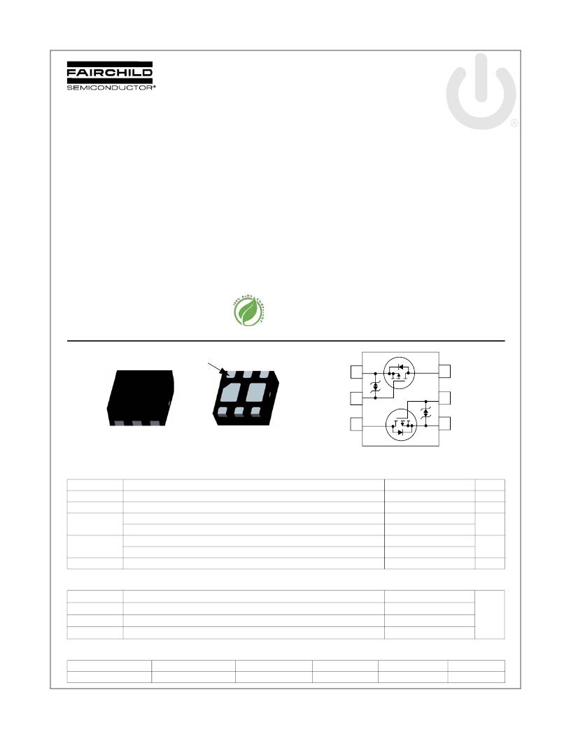
| 产品目录绘图: | MicorFET 2x2, SC-75 Dual |
| 标准包装: | 1 |
| 系列: | PowerTrench® |
| FET 型: | 2 个 P 沟道(双) |
| FET 特点: | 逻辑电平门 |
| 漏极至源极电压(Vdss): | 20V |
| 电流 - 连续漏极(Id) @ 25° C: | 3.6A |
| 开态Rds(最大)@ Id, Vgs @ 25° C: | 60 毫欧 @ 3.6A,4.5V |
| Id 时的 Vgs(th)(最大): | 1.5V @ 250µA |
| 闸电荷(Qg) @ Vgs: | 17nC @ 4.5V |
| 输入电容 (Ciss) @ Vds: | 885pF @ 10V |
| 功率 - 最大: | 700mW |
| 安装类型: | 表面贴装 |
| 封装/外壳: | 6-UDFN 裸露焊盘 |
| 供应商设备封装: | 6-MicroFET(2x2) |
| 包装: | 标准包装 |
| 其它名称: | FDMA6023PZTDKR |
�� �
�
�June� 2009�
�FDMA6023PZT�
�Dual� P-Channel� PowerTrench� ?� MOSFET�
�-20� V,� -3.6� A,� 60� m� ?�
�Features�
�Max� r� DS(on)� =� 60� m� ?� at� V� GS� =� -4.5� V,� I� D� =� -3.6� A�
�Max� r� DS(on)� =� 80� m� ?� at� V� GS� =� -2.5� V,� I� D� =� -3.0� A�
�Max� r� DS(on)� =� 110� m� ?� at� V� GS� =� -1.8� V,� I� D� =� -2.0� A�
�Max� r� DS(on)� =� 170� m� ?� at� V� GS� =� -1.5� V,� I� D� =� -1.0� A�
�Low� Profile-0.55� mm� maximum� -� in� the� new� package�
�MicroFET� 2x2� mm� Thin�
�HBM� ESD� protection� level� >� 2.4� kV� typical� (Note� 3)�
�RoHS� Compliant�
�General� Description�
�This� device� is� designed� specifically� as� a� single� package� solution�
�for� the� battery� charge� switch� in� cellular� handset� and� other�
�ultraportable� applications.� It� features� two� independent�
�P-Channel� MOSFETs� with� low� on-state� resistance� for� minimum�
�conduction� losses.� When� connected� in� the� typical� common�
�source� configuration,� bi-directional� current� flow� is� possible.�
�The� MicroFET� 2X2� Thin� package� offers� exceptional� thermal�
�performance� for� it’s� physical� size� and� is� well� suited� to� linear�
�mode� applications.�
�Applications�
�Free� from� halogenated� compounds� and� antimony� oxides�
�Battery� protection�
�Battery� management�
�Load� switch�
�Pin� 1�
�S1�
�G1�
�D2�
�S1�
�1�
�Q1�
�6�
�D1�
�D1�
�D2�
�G1�
�D2�
�2�
�3�
�5�
�4�
�G2�
�S2�
�D1�
�G2� S2�
�Q2�
�MicroFET� 2x2�
�MOSFET� Maximum� Ratings� T� A� =� 25� °C� unless� otherwise� noted�
�Symbol�
�V� DS�
�V� GS�
�Drain� to� Source� Voltage�
�Gate� to� Source� Voltage�
�Parameter�
�Ratings�
�-20�
�±8�
�Units�
�V�
�V�
�I� D�
�P� D�
�-Continuous�
�-Pulsed�
�Power� Dissipation�
�Power� Dissipation�
�T� A� =� 25� °C�
�T� A� =� 25� °C�
�T� A� =� 25� °C�
�(Note� 1a)�
�(Note� 1a)�
�(Note� 1b)�
�-3.6�
�-15�
�1.4�
�0.7�
�A�
�W�
�T� J� ,� T� STG�
�Operating� and� Storage� Junction� Temperature� Range�
�-55� to� +150�
�°C�
�Thermal� Characteristics�
�R� θ� JA�
�Thermal� Resistance� for� Single� Operation,� Junction� to� Ambient�
�(Note� 1a)�
�86�
�R� θ� JA�
�R� θ� JA�
�R� θ� JA�
�Thermal� Resistance� for� Single� Operation,� Junction� to� Ambient�
�Thermal� Resistance� for� Dual� Operation,� Junction� to� Ambient�
�Thermal� Resistance� for� Dual� Operation,� Junction� to� Ambient�
�(Note� 1b)�
�(Note� 1c)�
�(Note� 1d)�
�173�
�69�
�151�
�°C/W�
�Package� Marking� and� Ordering� Information�
�Device� Marking�
�623�
�Device�
�FDMA6023PZT�
�Package�
�MicroFET� 2X2� Thin�
�Reel� Size�
�7� ’’�
�Tape� Width�
�8mm�
�Quantity�
�3000� units�
�?2009� Fairchild� Semiconductor� Corporation�
�FDMA6023PZT� Rev.B1�
�1�
�www.fairchildsemi.com�
�相关PDF资料 |
PDF描述 |
|---|---|
| FDMA7630 | MOSFET N-CH 30V 6-MICROFET |
| FDMA7632 | MOSFET N-CH 30V 9A MICROFET2X2 |
| FDMA7670 | MOSFET N-CH 30V 6-MLP 2X2 |
| FDMA7672 | MOSFET N-CH 30V 6-MLP 2X2 |
| FDMA8884 | MOSFET N-CH 30V 6.5A 6-MLP 2X2 |
相关代理商/技术参数 |
参数描述 |
|---|---|
| FDMA7628 | 功能描述:MOSFET Snlg PT4, N 20/8V in MLP 2.05x2.05 RoHS:否 制造商:STMicroelectronics 晶体管极性:N-Channel 汲极/源极击穿电压:650 V 闸/源击穿电压:25 V 漏极连续电流:130 A 电阻汲极/源极 RDS(导通):0.014 Ohms 配置:Single 最大工作温度: 安装风格:Through Hole 封装 / 箱体:Max247 封装:Tube |
| FDMA7630 | 功能描述:MOSFET 30V Single N-Channel PowerTrench MOSFET RoHS:否 制造商:STMicroelectronics 晶体管极性:N-Channel 汲极/源极击穿电压:650 V 闸/源击穿电压:25 V 漏极连续电流:130 A 电阻汲极/源极 RDS(导通):0.014 Ohms 配置:Single 最大工作温度: 安装风格:Through Hole 封装 / 箱体:Max247 封装:Tube |
| FDMA7632 | 功能描述:MOSFET 30V Single N-Channel PowerTrench MOSFET RoHS:否 制造商:STMicroelectronics 晶体管极性:N-Channel 汲极/源极击穿电压:650 V 闸/源击穿电压:25 V 漏极连续电流:130 A 电阻汲极/源极 RDS(导通):0.014 Ohms 配置:Single 最大工作温度: 安装风格:Through Hole 封装 / 箱体:Max247 封装:Tube |
| FDMA7670 | 功能描述:MOSFET 30V Single N-Channel PowerTrench MOSFET RoHS:否 制造商:STMicroelectronics 晶体管极性:N-Channel 汲极/源极击穿电压:650 V 闸/源击穿电压:25 V 漏极连续电流:130 A 电阻汲极/源极 RDS(导通):0.014 Ohms 配置:Single 最大工作温度: 安装风格:Through Hole 封装 / 箱体:Max247 封装:Tube |
| FDMA7672 | 功能描述:MOSFET 30V Single N-Channel PowerTrench MOSFET RoHS:否 制造商:STMicroelectronics 晶体管极性:N-Channel 汲极/源极击穿电压:650 V 闸/源击穿电压:25 V 漏极连续电流:130 A 电阻汲极/源极 RDS(导通):0.014 Ohms 配置:Single 最大工作温度: 安装风格:Through Hole 封装 / 箱体:Max247 封装:Tube |
发布紧急采购,3分钟左右您将得到回复。