- 您现在的位置:买卖IC网 > Datasheet目录421 > FDMS3006SDC (Fairchild Semiconductor)MOSFET N-CH 30V 34A 8-PQFN Datasheet资料下载
参数资料
| 型号: | FDMS3006SDC |
| 厂商: | Fairchild Semiconductor |
| 文件页数: | 1/9页 |
| 文件大小: | 0K |
| 描述: | MOSFET N-CH 30V 34A 8-PQFN |
| 标准包装: | 3,000 |
| 系列: | Dual Cool™, PowerTrench®, SyncFET™ |
| FET 型: | MOSFET N 通道,金属氧化物 |
| FET 特点: | 逻辑电平门 |
| 漏极至源极电压(Vdss): | 30V |
| 电流 - 连续漏极(Id) @ 25° C: | 34A |
| 开态Rds(最大)@ Id, Vgs @ 25° C: | 1.9 毫欧 @ 30A,10V |
| Id 时的 Vgs(th)(最大): | 3V @ 1mA |
| 闸电荷(Qg) @ Vgs: | 80nC @ 10V |
| 输入电容 (Ciss) @ Vds: | 5725pF @ 15V |
| 功率 - 最大: | 3.3W |
| 安装类型: | 表面贴装 |
| 封装/外壳: | 8-PowerTDFN |
| 供应商设备封装: | Power56 |
| 包装: | 带卷 (TR) |
�� �
�
�July� 2013�
�FDMS3006SDC�
�N-Channel� Dual� Cool� TM� PowerTrench� ?� SyncFET� TM�
�30� V,� 90� A,� 1.9� m� Ω�
�Features�
�Dual� Cool� TM� Top� Side� Cooling� PQFN� package�
�Max� r� DS(on)� =� 1.9� m� Ω� at� V� GS� =� 10� V,� I� D� =� 30� A�
�Max� r� DS(on)� =� 2.7� m� Ω� at� V� GS� =� 4.5� V,� I� D� =� 26� A�
�High� performance� technology� for� extremely� low� r� DS(on)�
�SyncFET� Schottky� Body� Diode�
�RoHS� Compliant�
�General� Description�
�This� N-Channel� MOSFET� is� produced� using� Fairchild�
�Semiconductor’s� advanced� PowerTrench� ?� process.�
�Advancements� in� both� silicon� and� Dual� Cool� TM� package�
�technologies� have� been� combined� to� offer� the� lowest� r� DS(on)�
�while� maintaining� excellent� switching� performance� by� extremely�
�low� Junction-to-Ambient� thermal� resistance.� This� device� has� the�
�added� benefit� of� an� efficient� monolithic� Schottky� body� diode.�
�Applications�
�Synchronous� Rectifier� for� DC/DC� Converters�
�Telecom� Secondary� Side� Rectification�
�High� End� Server/Workstation� Vcore� Low� Side�
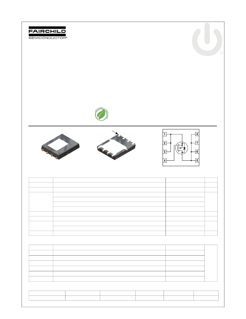
�D�
�D�
�Pin� 1�
�D�
�D�
�S�
�S�
�S�
�G�
�S�
�S�
�S�
�G�
�D�
�D�
�D�
�D�
�Top�
�Power� 56�
�Bottom�
�MOSFET� Maximum� Ratings� T� A� =� 25°C� unless� otherwise� noted�
�Symbol�
�V� DS�
�Drain� to� Source� Voltage�
�Parameter�
�Ratings�
�30�
�Units�
�V�
�V� GS�
�Gate� to� Source� Voltage�
�Drain� Current� -Continuous� (Package� limited)�
�T� C� =� 25� °C�
�(Note� 4)�
�±20�
�90�
�V�
�I� D�
�-Continuous� (Silicon� limited)�
�-Continuous�
�T� C� =� 25� °C�
�T� A� =� 25� °C�
�(Note� 1a)�
�179�
�34�
�A�
�-Pulsed�
�200�
�E� AS�
�dv/dt�
�Single� Pulse� Avalanche� Energy�
�Peak� Diode� Recovery� dv/dt�
�(Note� 3)�
�(Note� 5)�
�144�
�1.8�
�mJ�
�V/ns�
�P� D�
�Power� Dissipation�
�Power� Dissipation�
�T� C� =� 25� °C�
�T� A� =� 25� °C�
�(Note� 1a)�
�89�
�3.3�
�W�
�T� J� ,� T� STG�
�Operating� and� Storage� Junction� Temperature� Range�
�-55� to� +150�
�°C�
�Thermal� Characteristics�
�R� θ� JC�
�R� θ� JC�
�R� θ� JA�
�Thermal� Resistance,� Junction� to� Case�
�Thermal� Resistance,� Junction� to� Case�
�Thermal� Resistance,� Junction� to� Ambient�
�(Top� Source)�
�(Bottom� Drain)�
�(Note� 1a)�
�2.7�
�1.4�
�38�
�R� θ� JA�
�R� θ� JA�
�R� θ� JA�
�R� θ� JA�
�Thermal� Resistance,� Junction� to� Ambient�
�Thermal� Resistance,� Junction� to� Ambient�
�Thermal� Resistance,� Junction� to� Ambient�
�Thermal� Resistance,� Junction� to� Ambient�
�(Note� 1b)�
�(Note� 1i)�
�(Note� 1j)�
�(Note� 1k)�
�81�
�16�
�23�
�11�
�°C/W�
�Package� Marking� and� Ordering� Information�
�Device� Marking�
�3006S�
�Device�
�FDMS3006SDC�
�Package�
�Dual� Cool� TM� Power� 56�
�Reel� Size�
�13’’�
�Tape� Width�
�12� mm�
�Quantity�
�3000� units�
�?2012� Fairchild� Semiconductor� Corporation�
�FDMS3006SDC� Rev.C4�
�1�
�www.fairchildsemi.com�
�相关PDF资料 |
PDF描述 |
|---|---|
| FDMS3008SDC | MOSFET N-CH 30V 29A 8-PQFN |
| FDMS3016DC | MOSFET N-CH 30V 18A 8-PQFN |
| FDMS3500 | MOSFET N-CH 75V 9.2A POWER56 |
| FDMS3572 | MOSFET N-CH 80V 8.8A POWER56 |
| FDMS3600S | MOSFET N-CH 25V 15A 8-PQFN |
相关代理商/技术参数 |
参数描述 |
|---|---|
| FDMS3008SDC | 功能描述:MOSFET 30V N-Chan Dual Cool PowerTrench SyncFET RoHS:否 制造商:STMicroelectronics 晶体管极性:N-Channel 汲极/源极击穿电压:650 V 闸/源击穿电压:25 V 漏极连续电流:130 A 电阻汲极/源极 RDS(导通):0.014 Ohms 配置:Single 最大工作温度: 安装风格:Through Hole 封装 / 箱体:Max247 封装:Tube |
| FDMS3016DC | 功能描述:MOSFET 30V N-Channel Dual Cool PwrTrench RoHS:否 制造商:STMicroelectronics 晶体管极性:N-Channel 汲极/源极击穿电压:650 V 闸/源击穿电压:25 V 漏极连续电流:130 A 电阻汲极/源极 RDS(导通):0.014 Ohms 配置:Single 最大工作温度: 安装风格:Through Hole 封装 / 箱体:Max247 封装:Tube |
| FDMS3500 | 功能描述:MOSFET 75V N-Channel PowerTrench RoHS:否 制造商:STMicroelectronics 晶体管极性:N-Channel 汲极/源极击穿电压:650 V 闸/源击穿电压:25 V 漏极连续电流:130 A 电阻汲极/源极 RDS(导通):0.014 Ohms 配置:Single 最大工作温度: 安装风格:Through Hole 封装 / 箱体:Max247 封装:Tube |
| FDMS3572 | 功能描述:MOSFET 80V N-Ch UltraFET PowerTrench MOSFET RoHS:否 制造商:STMicroelectronics 晶体管极性:N-Channel 汲极/源极击穿电压:650 V 闸/源击穿电压:25 V 漏极连续电流:130 A 电阻汲极/源极 RDS(导通):0.014 Ohms 配置:Single 最大工作温度: 安装风格:Through Hole 封装 / 箱体:Max247 封装:Tube |
| FDMS3572_07 | 制造商:FAIRCHILD 制造商全称:Fairchild Semiconductor 功能描述:N-Channel UltraFET Trench㈢ MOSFET 80V, 22A, 16.5mз |
发布紧急采购,3分钟左右您将得到回复。