- 您现在的位置:买卖IC网 > PDF目录64933 > FSB50825US (FAIRCHILD SEMICONDUCTOR CORP) DC-DC REG PWR SUPPLY MODULE PDF资料下载
参数资料
| 型号: | FSB50825US |
| 厂商: | FAIRCHILD SEMICONDUCTOR CORP |
| 元件分类: | 电源模块 |
| 英文描述: | DC-DC REG PWR SUPPLY MODULE |
| 文件页数: | 3/8页 |
| 文件大小: | 297K |
| 代理商: | FSB50825US |
3
www.fairchildsemi.com
FSB50825US Rev. A
FSB50825US
Smart
Powe
rMod
u
le
(SPM)
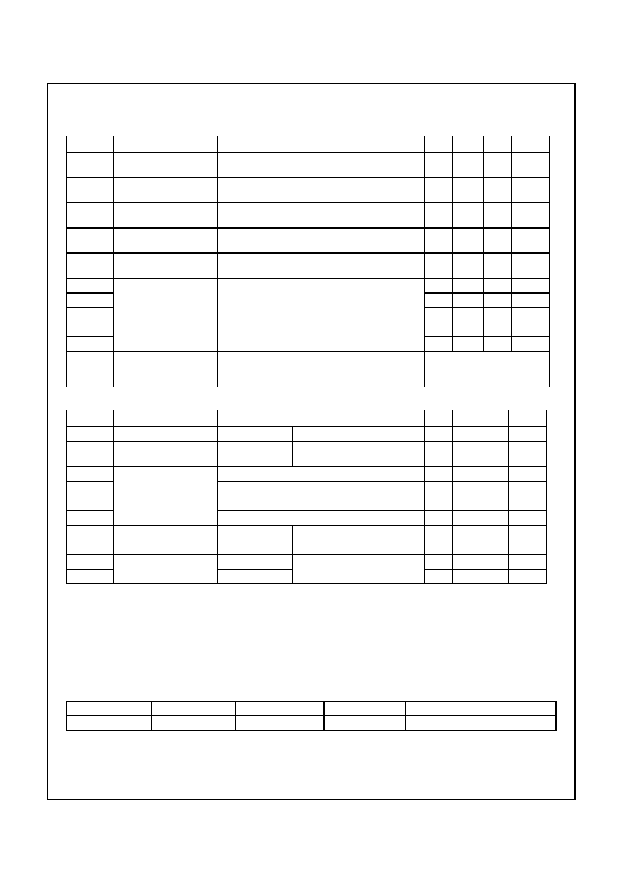
Electrical Characteristics (T
J = 25°C, VCC=VBS=15V Unless Otherwise Specified)
Inverter Part (Each FRFET Unless Otherwise Specified)
Control Part (Each HVIC Unless Otherwise Specified)
Note:
1. For the measurement point of case temperature TC, please refer to Figure 3 in page 4.
2. BVDSS is the absolute maximum voltage rating between drain and source terminal of each FRFET inside SPM
. V
PN should be sufficiently less than this value considering the
effect of the stray inductance so that VDS should not exceed BVDSS in any case.
3. tON and tOFF include the propagation delay time of the internal drive IC. Listed values are measured at the laboratory test condition, and they can be different according to the
field applcations due to the effect of different printed circuit boards and wirings. Please see Figure 4 for the switching time definition with the switching test circuit of Figure 5.
4. The peak current and voltage of each FRFET during the switching operation should be included in the safe operating area (SOA). Please see Figure 5 for the RBSOA test cir-
cuit that is same as the switching test circuit.
Package Marking & Ordering Information
Symbol
Parameter
Conditions
Min
Typ
Max
Units
BVDSS
Drain-Source Breakdown
Voltage
VIN= 0V, ID = 250μA (Note 2)
250
-
V
ΔBV
DSS/
ΔT
J
Breakdown Voltage Tem-
perature Coefficient
ID = 250μA, Referenced to 25°C
-
0.31
-
V
IDSS
Zero Gate Voltage
Drain Current
VIN= 0V, VDS = 250V
-
250
μA
RDS(on)
Static Drain-Source
On-Resistance
VCC = VBS = 15V, VIN = 5V, ID = 2.0A
-
0.45
Ω
VSD
Drain-Source Diode
Forward Voltage
VCC = VBS = 15V, VIN = 0V, ID = -2.0A
-
1.2
V
tON
Switching Times
VPN = 150V, VCC = VBS = 15V, ID = 2.0A
VIN = 0V 5V
Inductive load L=3mH
High- and low-side FRFET switching
(Note 3)
-
1050
-
ns
tOFF
-
450
-
ns
trr
-
140
-
ns
EON
-
100
-
μJ
EOFF
-
5
-
μJ
RBSOA
Reverse-bias Safe Oper-
ating Area
VPN = 200V, VCC = VBS = 15V, ID = IDP, VDS=BVDSS,
TJ = 150°C
High- and low-side FRFET switching (Note 4)
Full Square
Symbol
Parameter
Conditions
Min
Typ Max
Units
IQCC
Quiescent VCC Current
VCC=15V, VIN=0V Applied between VCC and COM
-
160
μA
IQBS
Quiescent VBS Current
VBS=15V, VIN=0V
Applied between VB(U)-U,
VB(V)-V, VB(W)-W
-
100
μA
UVCCD
Low-side Undervoltage
Protection (Figure 6)
VCC Undervoltage Protection Detection Level
7.4
8.0
9.4
V
UVCCR
VCC Undervoltage Protection Reset Level
8.0
8.9
9.8
V
UVBSD
High-side Undervoltage
Protection (Figure 7)
VBS Undervoltage Protection Detection Level
7.4
8.0
9.4
V
UVBSR
VBS Undervoltage Protection Reset Level
8.0
8.9
9.8
V
VIH
ON Threshold Voltage
Logic High Level
Applied between IN and COM
3.0
-
V
VIL
OFF Threshold Voltage
Logic Low Level
-
0.8
V
IIH
Input Bias Current
VIN = 5V
Applied between IN and COM
-
10
20
μA
IIL
VIN = 0V
-
2
μA
Device Marking
Device
Package
Reel Size
Packing Type
Quantity
FSB50825US
SPM23-BD
330mm
Tape & reel
450
相关PDF资料 |
PDF描述 |
|---|---|
| FSDS020-557GG | SIP20, IC SOCKET |
| FSG-15N1A | SPECIALTY ANALOG CIRCUIT, SSS4 |
| FSH2050A | PLL FREQUENCY SYNTHESIZER, QCC16 |
| FSH250300-100 | PLL FREQUENCY SYNTHESIZER, 150 MHz, QCC36 |
| FSH250300-1M | PLL FREQUENCY SYNTHESIZER, 3000 MHz, QCC36 |
相关代理商/技术参数 |
参数描述 |
|---|---|
| FSB52006S | 功能描述:IGBT 模块 60V 1A 15kHz RoHS:否 制造商:Infineon Technologies 产品:IGBT Silicon Modules 配置:Dual 集电极—发射极最大电压 VCEO:600 V 集电极—射极饱和电压:1.95 V 在25 C的连续集电极电流:230 A 栅极—射极漏泄电流:400 nA 功率耗散:445 W 最大工作温度:+ 125 C 封装 / 箱体:34MM 封装: |
| FSB560 | 功能描述:两极晶体管 - BJT NPN Transistor Low Saturation RoHS:否 制造商:STMicroelectronics 配置: 晶体管极性:PNP 集电极—基极电压 VCBO: 集电极—发射极最大电压 VCEO:- 40 V 发射极 - 基极电压 VEBO:- 6 V 集电极—射极饱和电压: 最大直流电集电极电流: 增益带宽产品fT: 直流集电极/Base Gain hfe Min:100 A 最大工作温度: 安装风格:SMD/SMT 封装 / 箱体:PowerFLAT 2 x 2 |
| FSB560_01 | 制造商:FAIRCHILD 制造商全称:Fairchild Semiconductor 功能描述:NPN Low Saturation Transistor |
| FSB560_Q | 功能描述:两极晶体管 - BJT NPN Transistor Low Saturation RoHS:否 制造商:STMicroelectronics 配置: 晶体管极性:PNP 集电极—基极电压 VCBO: 集电极—发射极最大电压 VCEO:- 40 V 发射极 - 基极电压 VEBO:- 6 V 集电极—射极饱和电压: 最大直流电集电极电流: 增益带宽产品fT: 直流集电极/Base Gain hfe Min:100 A 最大工作温度: 安装风格:SMD/SMT 封装 / 箱体:PowerFLAT 2 x 2 |
| FSB560A | 功能描述:两极晶体管 - BJT NPN Transistor Low Saturation RoHS:否 制造商:STMicroelectronics 配置: 晶体管极性:PNP 集电极—基极电压 VCBO: 集电极—发射极最大电压 VCEO:- 40 V 发射极 - 基极电压 VEBO:- 6 V 集电极—射极饱和电压: 最大直流电集电极电流: 增益带宽产品fT: 直流集电极/Base Gain hfe Min:100 A 最大工作温度: 安装风格:SMD/SMT 封装 / 箱体:PowerFLAT 2 x 2 |
发布紧急采购,3分钟左右您将得到回复。