- 您现在的位置:买卖IC网 > PDF目录370740 > HY5R288HC -|2.5V|8K|40|Direct RDRAM - 288M PDF资料下载
参数资料
| 型号: | HY5R288HC |
| 英文描述: | -|2.5V|8K|40|Direct RDRAM - 288M |
| 中文描述: | - |为2.5V | 8K的| 40 |直接RDRAM的- 288M |
| 文件页数: | 10/64页 |
| 文件大小: | 4542K |
| 代理商: | HY5R288HC |
第1页第2页第3页第4页第5页第6页第7页第8页第9页当前第10页第11页第12页第13页第14页第15页第16页第17页第18页第19页第20页第21页第22页第23页第24页第25页第26页第27页第28页第29页第30页第31页第32页第33页第34页第35页第36页第37页第38页第39页第40页第41页第42页第43页第44页第45页第46页第47页第48页第49页第50页第51页第52页第53页第54页第55页第56页第57页第58页第59页第60页第61页第62页第63页第64页
10
Rev.0.9/Dec.2000
Direct RDRAM
256/288-Mbit (512Kx16/18x32s) Preliminary
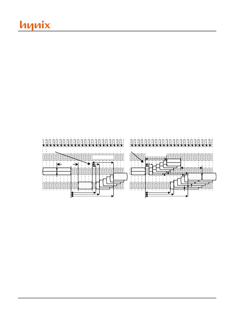
DQ Packet Timing
Figure 4: shows the timing relationship of COLC packets
with D and Q data packets. This document uses a specific
convention for measuring time intervals between packets: all
packets on the ROW and COL pins (ROWA, ROWR,
COLC, COLM, COLX) use the trailing edge of the packet as
a reference point, and all packets on the DQA/DQB pins (D
and Q) use the leading edge of the packet as a reference
point.
An RD or RDA command will transmit a dualoct of read
data Q a time t
CAC
later. This time includes one to five
cycles of round-trip propagation delay on the Channel. The
t
CAC
parameter may be programmed to a one of a range of
values ( 7, 8, 9, 10, 11, or 12 t
CYCLE
). The value chosen
depends upon the number of RDRAM devices on the
Channel and the RDRAM timing bin. See Figure 39: for
more information.
A WR or WRA command will receive a dualoct of write
data D a time t
CWD
later. This time does not need to include
the round-trip propagation time of the Channel since the
COLC and D packets are traveling in the same direction.
When a Q packet follows a D packet (shown in the left half
of the figure), a gap (t
CAC
-t
CWD
) will automatically appear
between them because the t
CWD
value is always less than the
t
CAC
value. There will be no gap between the two COLC
packets with the WR and RD commands which schedule the
D and Q packets.
When a D packet follows a Q packet (shown in the right half
of the figure), no gap is needed between them because the
t
CWD
value is less than the t
CAC
value. However, , a gap of
t
CAC
-t
CWD
or greater must be inserted between the COLC
packets with the RD WR commands by the controller so the
Q and D packets do not overlap.
COLM Packet to D Packet Mapping
Figure 5: shows a write operation initiated by a WR
command in a COLC packet. If a subset of the 16 bytes of
write data are to be written, then a COLM packet is trans-
mitted on the COL pins a time t
RTR
after the COLC packet
containing the WR command. The M bit of the COLM
packet is set to indicate that it contains the MA and MB
mask fields. Note that this COLM packet is aligned with the
COLC packet which causes the write buffer to be retired.
See Figure 17: for more details.
If all 16 bytes of the D data packet are to be written, then no
further control information is required. The packet slot that
would have been used by the COLM packet (t
RTR
after the
COLC packet) is available to be used as an COLX packet.
This could be used for a PREX precharge command or for a
housekeeping command (this case is not shown). The M bit
is not asserted in an COLX packet and causes all 16 bytes of
the previous WR to be written unconditionally. Note that a
RD command will never need a COLM packet, and will
always be able to use the COLX packet option (a read opera-
tion has no need for the byte-write-enable control bits).
Figure 5: also shows the mapping between the MA and MB
fields of the COLM packet and bytes of the D packet on the
DQA and DQB pins. Each mask bit controls whether a byte
of data is written (=1) or not written (=0).
Figure 4: Read (Q) and Write (D) Data Packet - Timing for t
CAC
= 7, 8, 9, 10, 11, or 12 t
CYCLE
CTM/CFM
DQA8..0
DQB8..0
COL4
..COL0
ROW2
..ROW0
T
0
T
4
T
8
T
12
T
1
T
5
T
9
T
13
T
2
T
6
T
10
T
14
T
3
T
7
T
11
T
15
T
16
T
20
T
24
T
28
T
17
T
21
T
25
T
29
T
18
T
22
T
26
T
30
T
19
T
23
T
27
T
31
T
32
T
36
T
40
T
44
T
33
T
37
T
41
T
45
T
34
T
38
T
42
T
46
T
35
T
39
T
43
T
47
D D (d1)
RD b1
Q Q (a1)
WR a1
D (a1)
t
CWD
RD c1
Q Q (a1)
t
CAC
-t
CWD
This gap on the DQA/DQB pins appears automatically
This gap on the COL pins must be inserted by the controller
t
CAC
-t
CWD
t
CAC
t
CAC
WWR d1
D (D (d1)
t
CWD
WWR d1
Q Q (c1)
WWR d1
D D (d1)
Q Q (c1)
Q Q (a1)
Q Q (b1)
相关PDF资料 |
PDF描述 |
|---|---|
| HY5V16CF | 1Mx16|3.3V|4K|H|SDR SDRAM - 16M |
| HY5V16CF-H | x16 SDRAM |
| HY5V16CF-S | x16 SDRAM |
| HY6116-10 | x8 SRAM |
| HY6116-12 | x8 SRAM |
相关代理商/技术参数 |
参数描述 |
|---|---|
| HY5S2B6DLF-BE | 制造商:HYNIX 制造商全称:Hynix Semiconductor 功能描述:4Banks x 2M x 16bits Synchronous DRAM |
| HY5S2B6DLFP-BE | 制造商:HYNIX 制造商全称:Hynix Semiconductor 功能描述:4Banks x 2M x 16bits Synchronous DRAM |
| HY5S2B6DLFP-SE | 制造商:HYNIX 制造商全称:Hynix Semiconductor 功能描述:4Banks x 2M x 16bits Synchronous DRAM |
| HY5S2B6DLF-SE | 制造商:HYNIX 制造商全称:Hynix Semiconductor 功能描述:4Banks x 2M x 16bits Synchronous DRAM |
| HY5S5B2BLF-6E | 制造商:HYNIX 制造商全称:Hynix Semiconductor 功能描述:256M (8Mx32bit) Mobile SDRAM |
发布紧急采购,3分钟左右您将得到回复。