- 您现在的位置:买卖IC网 > PDF目录370740 > HY5R288HC -|2.5V|8K|40|Direct RDRAM - 288M PDF资料下载
参数资料
| 型号: | HY5R288HC |
| 英文描述: | -|2.5V|8K|40|Direct RDRAM - 288M |
| 中文描述: | - |为2.5V | 8K的| 40 |直接RDRAM的- 288M |
| 文件页数: | 12/64页 |
| 文件大小: | 4542K |
| 代理商: | HY5R288HC |
第1页第2页第3页第4页第5页第6页第7页第8页第9页第10页第11页当前第12页第13页第14页第15页第16页第17页第18页第19页第20页第21页第22页第23页第24页第25页第26页第27页第28页第29页第30页第31页第32页第33页第34页第35页第36页第37页第38页第39页第40页第41页第42页第43页第44页第45页第46页第47页第48页第49页第50页第51页第52页第53页第54页第55页第56页第57页第58页第59页第60页第61页第62页第63页第64页
12
Rev.0.9/Dec.2000
Direct RDRAM
256/288-Mbit (512Kx16/18x32s) Preliminary
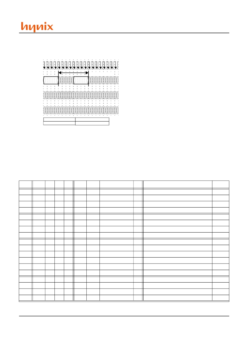
ROW-to-ROW Packet Interaction
Figure 6: shows two packets on the ROW pins separated by
an interval t
RRDELAY
which depends upon the packet
contents. No other ROW packets are sent to banks
{Ba,Ba+1,Ba-1} between packet “a” and packet “b” unless
noted otherwise. Table 9 summarizes the t
RRDELAY
values
for all possible cases.
Cases RR1 through RR4 show two successive ACT
commands. In case RR1, there is no restriction since the
ACT commands are to different devices. In case RR2, the
t
RR
restriction applies to the same device with non-adjacent
banks. Cases RR3 and RR4 are illegal (as shown) since bank
Ba needs to be precharged. If a PRER to Ba, Ba+1, or Ba-1
is inserted, t
RRDELAY
is t
RC
(t
RAS
to the PRER command,
and t
RP
to the next ACT).
Cases RR5 through RR8 show an ACT command followed
by a PRER command. In cases RR5 and RR6, there are no
restrictions since the commands are to different devices or to
non-adjacent banks of the same device. In cases RR7 and
RR8, the t
RAS
restriction means the activated bank must wait
before it can be precharged.
Cases RR9 through RR12 show a PRER command followed
by an ACT command. In cases RR9 and RR10, there are
essentially no restrictions since the commands are to
different devices or to non-adjacent banks of the same
device. RR10a and RR10b depend upon whether a bracketed
bank (Ba+-1) is precharged or activated. In cases RR11 and
RR12, the same and adjacent banks must all wait t
RP
for the
sense amp and bank to precharge before being activated.
Figure 6: ROW-to-ROW Packet Interaction- Timing
CTM/CFM
DQA8..0
DQB8..0
COL4
..COL0
ROW2
..ROW0
T
0
T
4
T
8
T
12
T
1
T
5
T
9
T
13
T
2
T
6
T
10
T
14
T
3
T
7
T
11
T
15
T
16
T
T
17
T
18
T
19
Transaction a: ROPa
Transaction b: ROPb
a0 = {Da,Ba,Ra}
b0= {Db,Bb,Rb}
t
RRDELAY
ROPa a0
ROPb b0
Table 9: ROW-to-ROW Packet Interaction - Rules
Case #
ROPa
Da
Ba
Ra
ROPb
Db
Bb
Rb
t
RRDELAY
Example
RR1
ACT
Da
Ba
Ra
ACT
/= Da
xxxx
x..x
t
PACKET
Figure 11:
RR2
ACT
Da
Ba
Ra
ACT
== Da
/= {Ba,Ba+1,Ba-1}
x..x
t
RR
Figure 11:
RR3
ACT
Da
Ba
Ra
ACT
== Da
== {Ba+1,Ba-1}
x..x
t
RC
- illegal unless PRER to Ba/Ba+1/Ba-1
Figure 10:
RR4
ACT
Da
Ba
Ra
ACT
== Da
== {Ba}
x..x
t
RC
- illegal unless PRER to Ba/Ba+1/Ba-1
Figure 10:
RR5
ACT
Da
Ba
Ra
PRER
/= Da
xxxx
x..x
t
PACKET
Figure 11:
RR6
ACT
Da
Ba
Ra
PRER
== Da
/= {Ba,Ba+1,Ba-1}
x..x
t
PACKET
Figure 11:
RR7
ACT
Da
Ba
Ra
PRER
== Da
== { Ba+1,Ba-1}
x..x
t
RAS
Figure 10:
RR8
ACT
Da
Ba
Ra
PRER
== Da
== {Ba}
x..x
t
RAS
Figure 15:
RR9
PRER
Da
Ba
Ra
ACT
/= Da
xxxx
x..x
t
PACKET
Figure 12:
RR10
PRER
Da
Ba
Ra
ACT
== Da
/= {Ba,Ba+-1,Ba+-2}
x..x
t
PACKET
Figure 12:
RR10a
PRER
Da
Ba
Ra
ACT
== Da
== {Ba+2}
x..x
t
PACKET
/t
RP
if Ba+1 is precharged/activated.
RR10b
PRER
Da
Ba
Ra
ACT
== Da
== {Ba-2}
x..x
t
PACKET
/t
RP
if Ba-1 is precharged/activated.
RR11
PRER
Da
Ba
Ra
ACT
== Da
== {Ba+1,Ba-1}
x..x
t
RP
Figure 10:
RR12
PRER
Da
Ba
Ra
ACT
== Da
== {Ba}
x..x
t
RP
Figure 10:
RR13
PRER
Da
Ba
Ra
PRER
/= Da
xxxx
x..x
t
PACKET
Figure 12:
RR14
PRER
Da
Ba
Ra
PRER
== Da
/= {Ba,Ba+1,Ba-1}
x..x
t
PP
Figure 12:
RR15
PRER
Da
Ba
Ra
PRER
== Da
== {Ba+1,Ba-1}
x..x
t
PP
Figure 12:
RR16
PRER
Da
Ba
Ra
PRER
== Da
== Ba
x..x
t
PP
Figure 12:
相关PDF资料 |
PDF描述 |
|---|---|
| HY5V16CF | 1Mx16|3.3V|4K|H|SDR SDRAM - 16M |
| HY5V16CF-H | x16 SDRAM |
| HY5V16CF-S | x16 SDRAM |
| HY6116-10 | x8 SRAM |
| HY6116-12 | x8 SRAM |
相关代理商/技术参数 |
参数描述 |
|---|---|
| HY5S2B6DLF-BE | 制造商:HYNIX 制造商全称:Hynix Semiconductor 功能描述:4Banks x 2M x 16bits Synchronous DRAM |
| HY5S2B6DLFP-BE | 制造商:HYNIX 制造商全称:Hynix Semiconductor 功能描述:4Banks x 2M x 16bits Synchronous DRAM |
| HY5S2B6DLFP-SE | 制造商:HYNIX 制造商全称:Hynix Semiconductor 功能描述:4Banks x 2M x 16bits Synchronous DRAM |
| HY5S2B6DLF-SE | 制造商:HYNIX 制造商全称:Hynix Semiconductor 功能描述:4Banks x 2M x 16bits Synchronous DRAM |
| HY5S5B2BLF-6E | 制造商:HYNIX 制造商全称:Hynix Semiconductor 功能描述:256M (8Mx32bit) Mobile SDRAM |
发布紧急采购,3分钟左右您将得到回复。