- 您现在的位置:买卖IC网 > PDF目录370740 > HY5R288HC -|2.5V|8K|40|Direct RDRAM - 288M PDF资料下载
参数资料
| 型号: | HY5R288HC |
| 英文描述: | -|2.5V|8K|40|Direct RDRAM - 288M |
| 中文描述: | - |为2.5V | 8K的| 40 |直接RDRAM的- 288M |
| 文件页数: | 15/64页 |
| 文件大小: | 4542K |
| 代理商: | HY5R288HC |
第1页第2页第3页第4页第5页第6页第7页第8页第9页第10页第11页第12页第13页第14页当前第15页第16页第17页第18页第19页第20页第21页第22页第23页第24页第25页第26页第27页第28页第29页第30页第31页第32页第33页第34页第35页第36页第37页第38页第39页第40页第41页第42页第43页第44页第45页第46页第47页第48页第49页第50页第51页第52页第53页第54页第55页第56页第57页第58页第59页第60页第61页第62页第63页第64页
Rev.0.9 / Dec.2000
15
Direct RDRAM
256/288-Mbit (512Kx16/18x32s) Preliminary
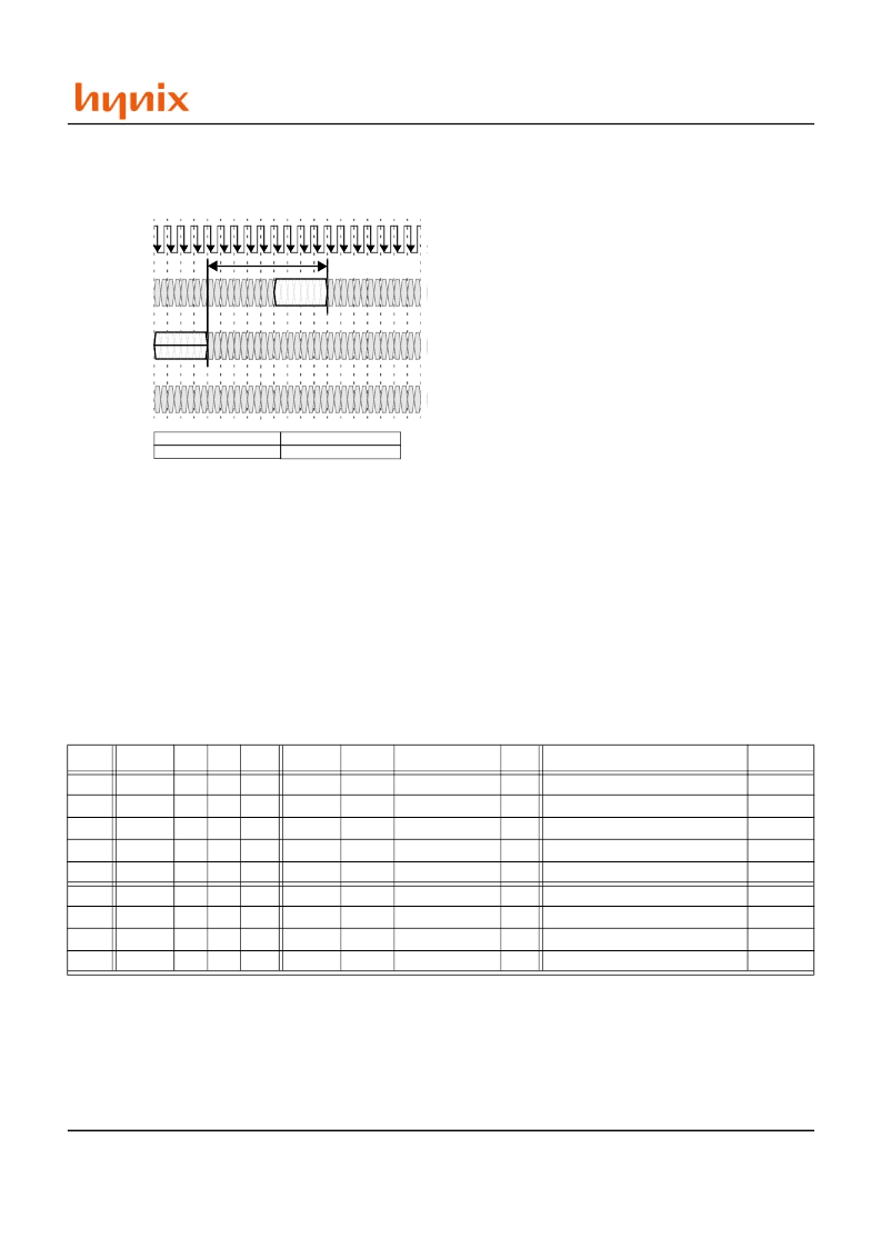
COL-to-ROW Packet Interaction
Figure 9: shows arbitrary packets on the COL and ROW
pins. They must be separated by an interval t
CRDELAY
which
depends upon the command and address values in the
packets. Table 12 summarizes the t
CRDELAY
value for all
possible cases.
Cases CR1, CR2, CR3, and CR9 show no interaction
between the COL and ROW packets, either because one of
the commands is a NOP or because the packets are directed
to different devices or to non-adjacent banks.
Case CR4 is illegal because an already-activated bank is to
be re-activated without being precharged Case CR5 is illegal
because an adjacent bank can’t be activated or precharged
until bank Ba is precharged first.
In case CR6, the COLC packet contains a RD command, and
the ROW packet contains a PRER command for the same
bank. The t
RDP
parameter specifies the required spacing.
Likewise, in case CR7, the COLC packet causes an auto-
matic retire to take place, and the ROW packet contains a
PRER command for the same bank. The t
RTP
parameter
specifies the required spacing.
Case CR8 is labeled “Hazardous” because a WR command
should always be followed by an automatic retire before a
precharge is scheduled. Figure 19: shows an example of
what can happen when the retire is not able to happen before
the precharge.
For the purposes of analyzing COL-to-ROW interactions,
the PREC, WRA, and RDA commands of the COLC packet
are equivalent to the NOCOP, WR, and RD commands.
These commands also cause a precharge operation to take
place. This precharge may converted to an equivalent PRER
command on the ROW pins using the rules summarized in
Figure 14:.
A ROW packet may contain commands other than ACT or
PRER. The REFA and REFP commands are equivalent to
ACT and PRER for interaction analysis purposes. The inter-
action rules of the NAPR, PDNR, and RLXR commands are
discussed in a later section.
Figure 9: COL-to-ROW Packet Interaction- Timing
CTM/CFM
DQA8..0
DQB8..0
COL4
..COL0
ROW2
..ROW0
T
0
T
4
T
8
T
12
T
1
T
5
T
9
T
13
T
2
T
6
T
10
T
14
T
3
T
7
T
11
T
15
T
16
T
T
17
T
18
T
19
Transaction a: COPa
Transaction b: ROPb
a1= {Da,Ba,Ca1}
b0= {Db,Bb,Rb}
t
CRDELAY
ROPb b0
COPa a1
Table 12: COL-to-ROW Packet Interaction - Rules
Case #
COPa
Da
Ba
Ca1
ROPb
Db
Bb
Rb
t
CRDELAY
Example
CR1
NOCOP
Da
Ba
Ca1
x..x
xxxxx
xxxx
x..x
0
CR2
RD/WR
Da
Ba
Ca1
x..x
/= Da
xxxx
x..x
0
CR3
RD/WR
Da
Ba
Ca1
x..x
== Da
/= {Ba,Ba+1,Ba-1}
x..x
0
CR4
RD/WR
Da
Ba
Ca1
ACT
== Da
== {Ba}
x..x
Illegal
CR5
RD/WR
Da
Ba
Ca1
x..x
== Da
== {Ba+1,Ba-1}
x..x
Illegal
CR6
RD
Da
Ba
Ca1
PRER
== Da
== {Ba,Ba+1,Ba-1}
x..x
t
RDP
Figure 15:
CR7
retire
a
Da
Ba
Ca1
PRER
== Da
== {Ba,Ba+1,Ba-1}
x..x
t
RTP
Figure 16:
CR8
WR
b
Da
Ba
Ca1
PRER
== Da
== {Ba,Ba+1,Ba-1}
x..x
0
Figure 19:
CR9
xxxx
Da
Ba
Ca1
NOROP
xxxxx
xxxx
x..x
0
a. This is any command which permits the write buffer of device Da to retire (see Table 7). “Ba” is the bank address in the write buffer.
b. This situation is hazardous because the write buffer will be left unretired while the targeted bank is precharged. See Figure 19:.
相关PDF资料 |
PDF描述 |
|---|---|
| HY5V16CF | 1Mx16|3.3V|4K|H|SDR SDRAM - 16M |
| HY5V16CF-H | x16 SDRAM |
| HY5V16CF-S | x16 SDRAM |
| HY6116-10 | x8 SRAM |
| HY6116-12 | x8 SRAM |
相关代理商/技术参数 |
参数描述 |
|---|---|
| HY5S2B6DLF-BE | 制造商:HYNIX 制造商全称:Hynix Semiconductor 功能描述:4Banks x 2M x 16bits Synchronous DRAM |
| HY5S2B6DLFP-BE | 制造商:HYNIX 制造商全称:Hynix Semiconductor 功能描述:4Banks x 2M x 16bits Synchronous DRAM |
| HY5S2B6DLFP-SE | 制造商:HYNIX 制造商全称:Hynix Semiconductor 功能描述:4Banks x 2M x 16bits Synchronous DRAM |
| HY5S2B6DLF-SE | 制造商:HYNIX 制造商全称:Hynix Semiconductor 功能描述:4Banks x 2M x 16bits Synchronous DRAM |
| HY5S5B2BLF-6E | 制造商:HYNIX 制造商全称:Hynix Semiconductor 功能描述:256M (8Mx32bit) Mobile SDRAM |
发布紧急采购,3分钟左右您将得到回复。