- 您现在的位置:买卖IC网 > PDF目录67681 > IBM25403GCX-3JC76C2 RISC PROCESSOR, PQFP16 PDF资料下载
参数资料
| 型号: | IBM25403GCX-3JC76C2 |
| 元件分类: | 微控制器/微处理器 |
| 英文描述: | RISC PROCESSOR, PQFP16 |
| 封装: | PLASTIC, QFP-160 |
| 文件页数: | 54/54页 |
| 文件大小: | 541K |
| 代理商: | IBM25403GCX-3JC76C2 |
第1页第2页第3页第4页第5页第6页第7页第8页第9页第10页第11页第12页第13页第14页第15页第16页第17页第18页第19页第20页第21页第22页第23页第24页第25页第26页第27页第28页第29页第30页第31页第32页第33页第34页第35页第36页第37页第38页第39页第40页第41页第42页第43页第44页第45页第46页第47页第48页第49页第50页第51页第52页第53页当前第54页
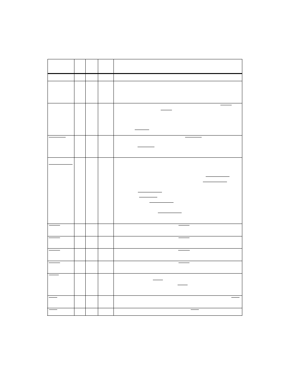
IBM PowerPC 403GCX
9
A29
119
C13
I/O
Address Bus Bit 29. See description of A22.
AMuxCAS
139
A8
O
DRAM External Address Multiplexer Select. AMuxCAS controls the
select logic on an external multiplexer. If AMuxCAS is low, the multi-
plexer should select the row address for the DRAM and when
AMuxCAS is 1, the multiplexer should select the column address.
BootW
11
E1
I
Boot-up ROM Width Select. BootW is sampled while the Reset pin
is active and again after Reset becomes inactive to determine the
width of the boot-up ROM. If this pin is tied to logic 0 when sampled
on reset, an 8-bit boot width is assumed. If BootW is tied to 1, a 32-
bit boot width is assumed. For 16-bit boot widths, this pin should be
tied to the RESET pin.
BusError
12
E3
I
Bus Error Input. A logic 0 input to the BusError pin by an external
device signals to the 403GCX that an error occurred on the bus
transaction. BusError is only sampled during the data transfer cycle
or the last wait cycle of the transfer.
BusReq/
DMADXFER
135
A9
O
Bus Request. While HoldAck is active, BusReq is active when the
403GCX has a bus operation pending and needs to regain control
of the bus.
DMA Data Transfer. When HoldAck is not active, DMADXFER indi-
cates a valid data transfer cycle. For DMA use, DMADXFER con-
trols burst-mode y-by DMA transfers between memory and
peripherals. DMADXFER is not meaningful unless a DMA Acknowl-
edge signal (DMAA0:3) is active. For transfer rates slower than one
transfer per cycle, DMADXFER is active for one cycle when one
transfer is complete and the next one starts. For transfer rates of
one transfer per cycle, DMADXFER remains active throughout the
transfer.
CAS0
142
C8
O
DRAM Column Address Select 0. CAS0 is used with byte 0 of all
DRAM banks.
CAS1
143
A7
O
DRAM Column Address Select 1. CAS1 is used with byte 1 of all
DRAM banks.
CAS2
144
B7
O
DRAM Column Address Select 2. CAS2 is used with byte 2 of all
DRAM banks.
CAS3
145
D7
O
DRAM Column Address Select 3. CAS3 is used with byte 3 of all
DRAM banks.
CINT
36
L2
I
Critical Interrupt. To initiate a critical interrupt, the user must main-
tain a logic 0 on the CINT pin for a minimum of one SysClk clock
cycle followed by a logic 1 on the CINT pin for at least one SysClk
cycle.
CS0
155
C4
O
SRAM Chip Select 0. Bank register 0 controls an SRAM bank, CS0
is the chip select for that bank.
CS1
154
A4
O
SRAM Chip Select 1. See description of CS0 but controls bank 1.
Table 4. 403GCX Signal Descriptions
Signal
Name
Pin
Ball
I/O
Type
Function
相关PDF资料 |
PDF描述 |
|---|---|
| IBM25405GP-3BA200C2 | RISC PROCESSOR, PBGA456 |
| IBM25EMPPC603EFG-100 | 32-BIT, 100 MHz, RISC PROCESSOR, PQFP240 |
| IBM25EMPPC603EBG-100 | 32-BIT, 100 MHz, RISC PROCESSOR, CBGA255 |
| IBM25EMPPC740LDBC4000 | 32-BIT, 400 MHz, RISC PROCESSOR, CBGA255 |
| IBM25EMPPC750LCBF3330 | 32-BIT, 333 MHz, RISC PROCESSOR, CBGA360 |
相关代理商/技术参数 |
参数描述 |
|---|---|
| IBM25403GCX-JA50C2 | 制造商:IBM 功能描述:403GCX-JA50C |
| IBM25403GCX-JA60C2 | 制造商:IBM 功能描述:403GCX-JA60C2 |
| IBM25C710AB3A100 | 制造商:未知厂家 制造商全称:未知厂家 功能描述:Controller Miscellaneous - Datasheet Reference |
| IBM25CPC700BB3B66 | 制造商:未知厂家 制造商全称:未知厂家 功能描述:Peripheral (Multifunction) Controller |
| IBM25CPC700BB3B83 | 制造商:未知厂家 制造商全称:未知厂家 功能描述:Peripheral (Multifunction) Controller |
发布紧急采购,3分钟左右您将得到回复。