- 您现在的位置:买卖IC网 > PDF目录67682 > IBM25PPC405GP-3DE266CZ 32-BIT, 266.66 MHz, RISC PROCESSOR, PBGA456 PDF资料下载
参数资料
| 型号: | IBM25PPC405GP-3DE266CZ |
| 元件分类: | 微控制器/微处理器 |
| 英文描述: | 32-BIT, 266.66 MHz, RISC PROCESSOR, PBGA456 |
| 封装: | 27 X 27 MM, ENHANCED, PLASTIC, BGA-456 |
| 文件页数: | 31/60页 |
| 文件大小: | 1480K |
| 代理商: | IBM25PPC405GP-3DE266CZ |
第1页第2页第3页第4页第5页第6页第7页第8页第9页第10页第11页第12页第13页第14页第15页第16页第17页第18页第19页第20页第21页第22页第23页第24页第25页第26页第27页第28页第29页第30页当前第31页第32页第33页第34页第35页第36页第37页第38页第39页第40页第41页第42页第43页第44页第45页第46页第47页第48页第49页第50页第51页第52页第53页第54页第55页第56页第57页第58页第59页第60页
PowerPC 405GP Embedded Processor Data Sheet
6/20/03
Page 37 of 60
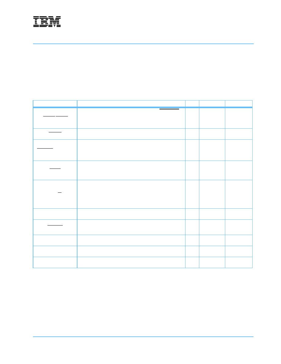
[PerWE]PCIINT
Peripheral write enable. Low when any of the four PerWBE0:3
write byte enables are low.
or
PCI interrupt. Open-drain output (two states; 0 or open circuit)
O
5V tolerant
3.3V PCI
PerCS0
Peripheral chip select bank 0.
O
5V tolerant
3.3V LVTTL
7
PerCS1:7[GPIO10:16]
Seven additional peripheral chip selects
or
General Purpose I/O. To access this function, software must
toggle a DCR bit.
O[I/O]
5V tolerant
3.3V LVTTL
1, 7
PerOE
Used by either the peripheral controller or the DMA controller
depending upon the type of transfer involved. When the
PPC405GP is the bus master, it enables the selected device to
drive the bus.
O
5V tolerant
3.3V LVTTL
7
PerR/W
Used by the PPC405GP when not in external master mode, as
output by either the peripheral controller or DMA controller
depending upon the type of transfer involved. High indicates a
read from memory, low indicates a write to memory.
Otherwise it used by the external master as an input to indicate
the direction of data transfer.
I/O
5V tolerant
3.3V LVTTL
1
PerReady
Used by a peripheral slave to indicate it is ready to transfer data.
I
5V tolerant
3.3V LVTTL
1
PerBLast
Used by the PPC405GP when not in external master mode,
otherwise used by external master. Indicates the last transfer of a
memory access.
I/O
5V tolerant
3.3V LVTTL
1, 7
DMAReq0:3
DMAReq0:3 are used by slave peripherals to indicate they are
prepared to transfer data.
I
5V tolerant
3.3V LVTTL
1
DMAAck0:3
DMAAck0:3 are used by the PPC405GP to cause the DMA
peripheral to transfer data.
O
5V tolerant
3.3V LVTTL
6
EOT0:3/TC0:3
End Of Transfer/Terminal Count.
I/O
5V tolerant
3.3V LVTTL
1
Signal Functional Description (Part 4 of 8)
Multiplexed signals are shown in brackets following the first signal name assigned to each multiplexed ball.
Notes:
1. Receiver input has hysteresis.
2. Must pull up. See “Pull-Up and Pull-Down Resistors” on page 33 for recommended termination values.
3. Must pull down. See “Pull-Up and Pull-Down Resistors” on page 33 for recommended termination values.
4. If not used, must pull up.
5. If not used, must pull down.
6. Strapping input during reset; pull up or pull down as required.
7. Pull-up may be required. See “External Bus Control Signals” on page 33.
Signal Name
Description
I/O
Type
Notes
相关PDF资料 |
PDF描述 |
|---|---|
| IBM25PPC405GP-3BE133C | 32-BIT, 133.33 MHz, RISC PROCESSOR, PBGA456 |
| IBM25PPC405GPR-3BA333CZ | 32-BIT, 333 MHz, RISC PROCESSOR, PBGA456 |
| IBM25PPC405GPR3DB400Z | 32-BIT, 400 MHz, RISC PROCESSOR, PBGA456 |
| IBM25PPC405GPR3BB400Z | 32-BIT, 400 MHz, RISC PROCESSOR, PBGA456 |
| IBM25PPC405GPR3DB266 | 32-BIT, 266 MHz, RISC PROCESSOR, PBGA456 |
相关代理商/技术参数 |
参数描述 |
|---|---|
| IBM25PPC405GP-3EE200C | 制造商:未知厂家 制造商全称:未知厂家 功能描述:MICROPROCESSOR|32-BIT|CMOS|BGA|413PIN|PLASTIC |
| IBM25PPC405GP3EE200CZ | 制造商:未知厂家 制造商全称:未知厂家 功能描述:MICROPROCESSOR|32-BIT|CMOS|BGA|413PIN|PLASTIC |
| IBM25PPC405GP-3EE266C | 制造商:未知厂家 制造商全称:未知厂家 功能描述:MICROPROCESSOR|32-BIT|CMOS|BGA|413PIN|PLASTIC |
| IBM25PPC405GP3EE266CZ | 制造商:IBM 功能描述: |
| IBM25PPC405GPR3BB266 | 制造商:IBM 功能描述: |
发布紧急采购,3分钟左右您将得到回复。