- 您现在的位置:买卖IC网 > PDF目录67704 > ICS9148F-14LF 66.6 MHz, PROC SPECIFIC CLOCK GENERATOR, PDSO48 PDF资料下载
参数资料
| 型号: | ICS9148F-14LF |
| 元件分类: | 时钟产生/分配 |
| 英文描述: | 66.6 MHz, PROC SPECIFIC CLOCK GENERATOR, PDSO48 |
| 封装: | 0.300 INCH, SSOP-48 |
| 文件页数: | 1/18页 |
| 文件大小: | 807K |
| 代理商: | ICS9148F-14LF |
Integrated
Circuit
Systems, Inc.
General Description
Features
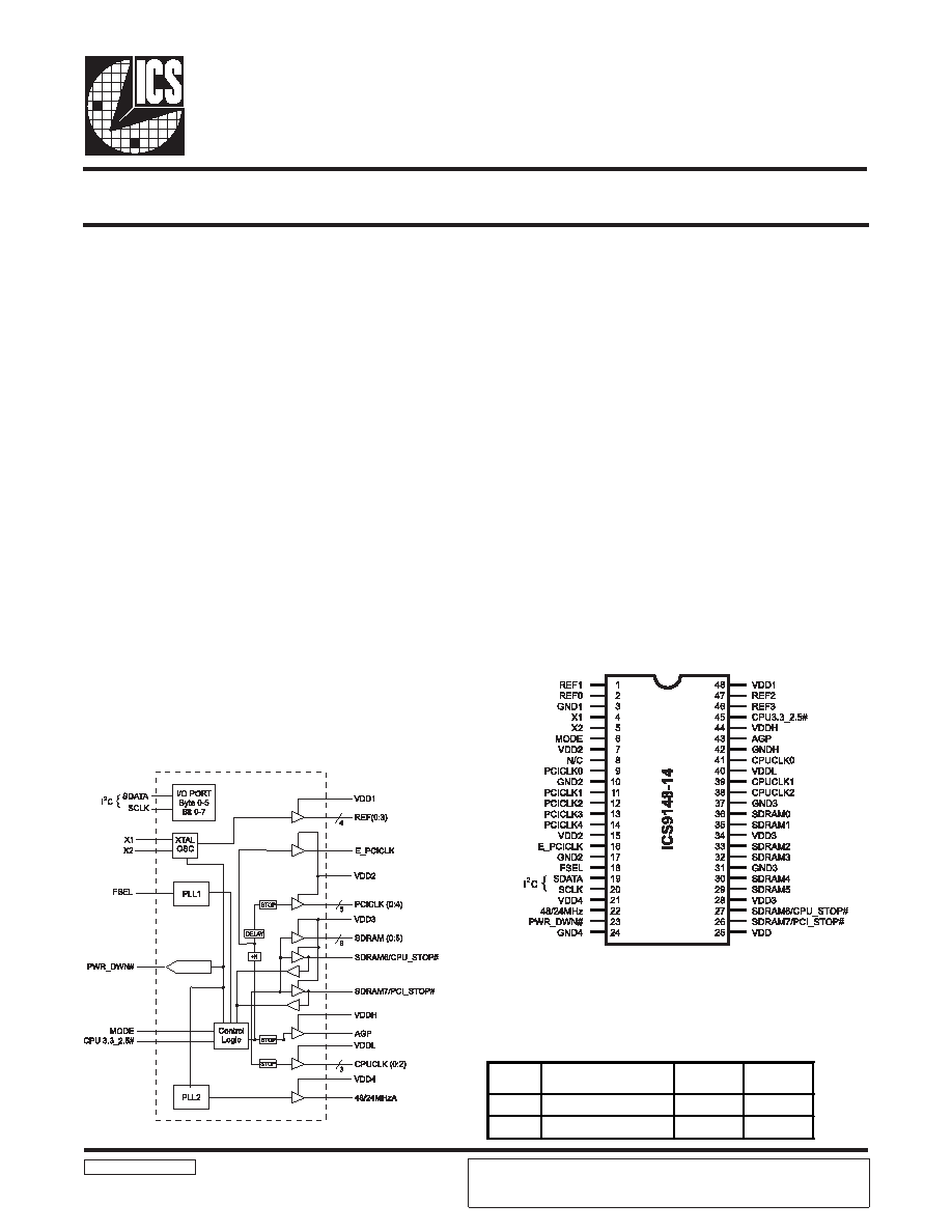
ICS9148-14
Block Diagram
Pentium/ProTM Clock Chip for Mobile/Docking Systems
9148-14 Rev B 02/20/98
Pentium is a trademark of Intel Corporation.
Generates system clocks for CPU,AGP, SDRAM, PCI,
plus 14.314 MHz REF(0:3), USB, or Super I/O
Skew defined for Mobile/Docking Station use
I2C serial configuration interface provides output clock
disabling and other functions
MODE input pin selects optional power management
input control pins
Fixed output separately selectable as 24 or 48MHz
Separate 2.5V and 3.3V supply pins
2.5V or 3.3V outputs: CPU
3.3Voutputs: SDRAM, PCI, REF, 48/24 MHz,AGP
CPU 3.3_2.5# logic pin to adjust output strength
No power supply sequence requirements
Uses external 14.318MHz crystal
48pin300milSSOP
I2C pins 5V input tolerant
The ICS9148-14 is a Clock Synthesizer chip for Pentium and
PentiumPro CPU based Mobile/Docking systems that will
provide all necessary clock timing.
Features include three CPU, oneAGP, early PCI, five PCI and
eight SDRAM clocks. Four reference outputs are available
equal to the crystal frequency. The single AGP output is
defined as 2X the PCI BUS speed. For Mobile Docking station
the Early PCI is 1.5ns ±250ps leading the PCI (0:4). SDRAM
leads CPU by 1.2ns ±250ps. CPU to PCI (0:4) skew is 500ps
max.
PWR_DWN# pin allows low power mode by stopping crystal
OSC and PLL stages. For optional power management,
CPU_STOP# can stop CPU (0:2) clocks, PCI_STOP# will stop
E_PCICLK, PCICLK (0:4) andAGPclocks. Both low will also
stop SDRAM outputs. CPU output buffer strength is controlled
by the CPU 3.3_2.5# pin to match VDDL voltage.
High drive CPUCLK outputs typically provide greater than 1
V/ns slew rate into 20pF loads. SDRAM outputs typically
provide better than 1V/ns slew rate into 30pF loads while
maintaining50±5% duty cycle. The REF clock outputs typically
providebetterthan0.5V/nsslewrates,REF0into47pF,REF(1:3)
into 20pF loads. PCI outputs are sized for EMI imporvement,
providing 0.5v/ns slew rate into 20pF.
The ICS9148-14 accepts a 14.318MHz reference crystal or
clock as its input and runs on a 3.3V core supply.
Functionality
VDD(1:4)3.3V±5%,VDDL1,22.5±5%or3.3±5%0-70°C
Crystal (X1, X2) = 14.31818 MHz
Pin Configuration
48-Pin SSOP
SEL
CPUCLK, SDRAM
(MHz)
PCICLK
(MHz)
AGP
(MHz)
0
Reserved
-
1
66.6
33.3
66.6
ICS reserves the right to make changes in the device data identified in this
publication without further notice. ICS advises its customers to obtain the latest
version of all device data to verify that any information being relied upon by the
customer is current and accurate.
相关PDF资料 |
PDF描述 |
|---|---|
| ICS9148F-14 | 66.6 MHz, PROC SPECIFIC CLOCK GENERATOR, PDSO48 |
| ICS9148F-17-LF | 100.3569 MHz, PROC SPECIFIC CLOCK GENERATOR, PDSO48 |
| ICS9148F-17 | 100.3569 MHz, PROC SPECIFIC CLOCK GENERATOR, PDSO48 |
| ICS9148F-18LF | 100 MHz, PROC SPECIFIC CLOCK GENERATOR, PDSO28 |
| ICS9148F-25 | 83.3 MHz, PROC SPECIFIC CLOCK GENERATOR, PDSO48 |
相关代理商/技术参数 |
参数描述 |
|---|---|
| ICS9148F-17 | 制造商:未知厂家 制造商全称:未知厂家 功能描述:CPU System Clock Generator |
| ICS9148F-18 | 制造商:ICS 制造商全称:ICS 功能描述:Pentium/ProTM System Clock Chip |
| ICS9148F-20 | 制造商:ICS 制造商全称:ICS 功能描述:Pentium/ProTM System Clock Chip |
| ICS9148F25 | 制造商:未知厂家 制造商全称:未知厂家 功能描述:Industrial Control IC |
| ICS9148F-25 | 功能描述:IC CLK SYNTHESIZER CHIP 48-SSOP RoHS:否 类别:集成电路 (IC) >> 时钟/计时 - 专用 系列:- 标准包装:28 系列:- 类型:时钟/频率发生器 PLL:是 主要目的:Intel CPU 服务器 输入:时钟 输出:LVCMOS 电路数:1 比率 - 输入:输出:3:22 差分 - 输入:输出:无/是 频率 - 最大:400MHz 电源电压:3.135 V ~ 3.465 V 工作温度:0°C ~ 85°C 安装类型:表面贴装 封装/外壳:64-TFSOP (0.240",6.10mm 宽) 供应商设备封装:64-TSSOP 包装:管件 |
发布紧急采购,3分钟左右您将得到回复。