- 您现在的位置:买卖IC网 > PDF目录1999 > ICS9FG1901HKLFT (IDT, Integrated Device Technology Inc)IC FREQUENCY GENERATOR 72-QFN PDF资料下载
参数资料
| 型号: | ICS9FG1901HKLFT |
| 厂商: | IDT, Integrated Device Technology Inc |
| 文件页数: | 5/18页 |
| 文件大小: | 0K |
| 描述: | IC FREQUENCY GENERATOR 72-QFN |
| 标准包装: | 1 |
| 系列: | PCI Express® (PCIe) |
| 类型: | 时钟/频率发生器 |
| PLL: | 是 |
| 主要目的: | 存储器,DIMM,PCI Express(PCIe) |
| 输入: | HCSL |
| 输出: | HCSL |
| 电路数: | 1 |
| 比率 - 输入:输出: | 1:19 |
| 差分 - 输入:输出: | 是/是 |
| 频率 - 最大: | 400MHz |
| 电源电压: | 3.135 V ~ 3.465 V |
| 工作温度: | 0°C ~ 70°C |
| 安装类型: | 表面贴装 |
| 封装/外壳: | 72-VFQFN 裸露焊盘 |
| 供应商设备封装: | 72-VFQFPN(10x10) |
| 包装: | 标准包装 |
| 产品目录页面: | 1251 (CN2011-ZH PDF) |
| 其它名称: | 800-1264-6 |
IDTTM
Frequency Gearing Clock for CPU, PCIe Gen1 & FBD
1386A - 02/02/10
9FG1901H
Frequency Gearing Clock for CPU, PCIe Gen1 & FBD
13
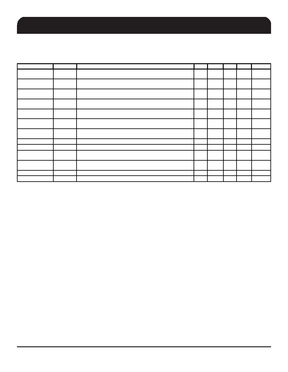
Electrical Characteristics - Skew and Differential Jitter Parameters
TA = 0 - 70°C; Supply Voltage VDD = 3.3 V +/-5%
Group
Parameter
Description
Min
Typ
Max
Units
Notes
CLK_IN, DIF[x:0]
tSPO_PLL
Input-to-Output Skew in PLL mode (1:1 only),
nominal value @ 25°C, 3.3V
-500
270
500
ps
1,2,4,5,8,
12
CLK_IN, DIF[x:0]
tPD_BYP
Input-to-Output Skew in Bypass mode (1:1 only),
nominal value @ 25°C, 3.3V
2.5
3.8
4.5
ns
1,2,3,5,
12
CLK_IN, DIF [x:0]
tSPO_PLL
Input-to-Output Skew Variation in PLL mode
(over specified voltage / temperature operating ranges)
270
|500|
ps
1,2,4,5,6,
10,12
CLK_IN, DIF [x:0]
tPD_BYP
Input-to-Output Skew Variation in Bypass mode
(over specified voltage / temperature operating ranges)
467
|500|
ps
1,2,3,4,5,
6,10,12
DIF[18:17]
tSKEW_G2
Output-to-Output Skew Group of 2
(Common to Bypass and PLL mode)
10
50
ps
1,2,12
DIF[16:0]
tSKEW_G17
Output-to-Output Skew Group of 17
(Common to Bypass and PLL mode)
70
100
ps
1,2,12
DIF[18:0]
tSKEW_A19
Output-to-Output Skew across all 19 outputs (Common to
Bypass and PLL mode - all outputs at same gear)
70
150
ps
1,2,3,12
DIF[18:0]
tJPH
Differential Phase Jitter (RMS Value)
5
10
ps
1,4,7,12
DIF[18:0]
tSSTERROR
Differential Spread Spectrum Tracking Error (peak to peak)
40
80
ps
1,4,9,12
PLL Jitter Peaking
jpeak-hibw
(HIGH_BW# = 0)
0
2.2
2.5
dB
11,12
PLL Jitter Peaking
jpeak-lobw
(HIGH_BW# = 1)
0
1.4
2
dB
11,12
PLL Bandwidth
pllHIBW
(HIGH_BW# = 0)
2
3.7
4
MHz
12,13
PLL Bandwidth
pllLOBW
(HIGH_BW# = 1)
0.7
1.2
1.4
MHz
12,13
NOTES on Skew and Differential Jitter Parameters:
8. t is the period of the input clock
11. Measured as maximum pass band gain. At frequencies w ithin the loop BW, highest point of magnification is called PLL jitter peaking.
12. Guaranteed by design and characterization, not 100% tested in production.
13. Measured at 3 db dow n or half pow er point.
3. All Bypass Mode Input-to-Output specs refer to the timing between an input edge and the specific output edge created by it.
4. This parameter is deterministic for a given device
1. Measured into fixed 2 pF load cap. Input to output skew is measured at the first output edge following the corresponding input.
2. Measured from differential cross-point to differential cross-point
10. This parameter is an absolute value. It is not a double-sided figure.
9. Differential spread spectrum tracking error is the difference in spread spectrum tracking betw een tw o 9FG1901H devices This parameter is measured at the
outputs of tw o separate 9FG1901H devices driven by a single CK410B+ in Spread Spectrum mode. The 9FG1901H must set to high bandw idth. The spread
spectrum characterisitics are : maximum of 0.5%, 30 to 33KHz modulation frequency, linear profile.
5. Measured with scope averaging on to find mean value.
6. Long-term variation from nominal of input-to-output skew over temperature and voltage for a single device.
7. This parameter is measured at the outputs of two separate 9FG1901H devices driven by a single CK410B+. The 9FG1901H must be set to high bandwidth.
Differential phase jitter is the accumulation of the phase jitter not shared by the outputs (eg. not including the affects of spread spectrum). Target ranges of
consideration are agents with BW of 1-22MHz and 11-33MHz.
相关PDF资料 |
PDF描述 |
|---|---|
| ID82C54 | IC OSC PROG TIMER 8MHZ 24DIP |
| IDT2308A-4DCI8 | IC CLOCK MULT ZD HI DRV 16-SOIC |
| IDT2309-1HPGGI | IC CLK BUFFER ZD HI DRV 16-TSSOP |
| IDT2309A-1HPGG | IC CLK BUFFER ZD HI DRV 16-TSSOP |
| IDT2309B-1HPGGI | IC CLK BUFFER HIGH DRIVE 16TSSOP |
相关代理商/技术参数 |
参数描述 |
|---|---|
| ICS9FG1902AKLF | 功能描述:IC FREQUENCY GENERATOR 72-VFQFPN RoHS:是 类别:集成电路 (IC) >> 时钟/计时 - 专用 系列:PCI Express® (PCIe) 标准包装:1,500 系列:- 类型:时钟缓冲器/驱动器 PLL:是 主要目的:- 输入:- 输出:- 电路数:- 比率 - 输入:输出:- 差分 - 输入:输出:- 频率 - 最大:- 电源电压:3.3V 工作温度:0°C ~ 70°C 安装类型:表面贴装 封装/外壳:28-SSOP(0.209",5.30mm 宽) 供应商设备封装:28-SSOP 包装:带卷 (TR) 其它名称:93786AFT |
| ICS9FG1902AKLFT | 功能描述:IC FREQUENCY GENERATOR 72-VFQFPN RoHS:是 类别:集成电路 (IC) >> 时钟/计时 - 专用 系列:PCI Express® (PCIe) 标准包装:1,500 系列:- 类型:时钟缓冲器/驱动器 PLL:是 主要目的:- 输入:- 输出:- 电路数:- 比率 - 输入:输出:- 差分 - 输入:输出:- 频率 - 最大:- 电源电压:3.3V 工作温度:0°C ~ 70°C 安装类型:表面贴装 封装/外壳:28-SSOP(0.209",5.30mm 宽) 供应商设备封装:28-SSOP 包装:带卷 (TR) 其它名称:93786AFT |
| ICS9FG1903AK-1LF | 功能描述:IC BUFFER PCIE 3.3V 72-VFQFPN RoHS:是 类别:集成电路 (IC) >> 时钟/计时 - 时钟发生器,PLL,频率合成器 系列:- 标准包装:1,000 系列:- 类型:时钟/频率合成器,扇出分配 PLL:- 输入:- 输出:- 电路数:- 比率 - 输入:输出:- 差分 - 输入:输出:- 频率 - 最大:- 除法器/乘法器:- 电源电压:- 工作温度:- 安装类型:表面贴装 封装/外壳:56-VFQFN 裸露焊盘 供应商设备封装:56-VFQFP-EP(8x8) 包装:带卷 (TR) 其它名称:844S012AKI-01LFT |
| ICS9FG1903AK-1LFT | 功能描述:IC BUFFER PCIE 3.3V 72-VFQFPN RoHS:是 类别:集成电路 (IC) >> 时钟/计时 - 时钟发生器,PLL,频率合成器 系列:- 标准包装:2,000 系列:- 类型:PLL 时钟发生器 PLL:带旁路 输入:LVCMOS,LVPECL 输出:LVCMOS 电路数:1 比率 - 输入:输出:2:11 差分 - 输入:输出:是/无 频率 - 最大:240MHz 除法器/乘法器:是/无 电源电压:3.135 V ~ 3.465 V 工作温度:0°C ~ 70°C 安装类型:表面贴装 封装/外壳:32-LQFP 供应商设备封装:32-TQFP(7x7) 包装:带卷 (TR) |
| ICS9FG1903AKLF | 功能描述:IC BUFFER PCIE 3.3V 72-VFQFPN RoHS:是 类别:集成电路 (IC) >> 时钟/计时 - 时钟发生器,PLL,频率合成器 系列:- 标准包装:1,000 系列:- 类型:时钟/频率合成器,扇出分配 PLL:- 输入:- 输出:- 电路数:- 比率 - 输入:输出:- 差分 - 输入:输出:- 频率 - 最大:- 除法器/乘法器:- 电源电压:- 工作温度:- 安装类型:表面贴装 封装/外壳:56-VFQFN 裸露焊盘 供应商设备封装:56-VFQFP-EP(8x8) 包装:带卷 (TR) 其它名称:844S012AKI-01LFT |
发布紧急采购,3分钟左右您将得到回复。