- 您现在的位置:买卖IC网 > PDF目录9942 > IDT72V3676L10PF8 (IDT, Integrated Device Technology Inc)IC FIFO 16384X36 10NS 128QFP PDF资料下载
参数资料
| 型号: | IDT72V3676L10PF8 |
| 厂商: | IDT, Integrated Device Technology Inc |
| 文件页数: | 5/39页 |
| 文件大小: | 0K |
| 描述: | IC FIFO 16384X36 10NS 128QFP |
| 标准包装: | 1,000 |
| 系列: | 72V |
| 功能: | 异步 |
| 存储容量: | 576K(16K x 36) |
| 数据速率: | 100MHz |
| 访问时间: | 10ns |
| 电源电压: | 3.15 V ~ 3.45 V |
| 工作温度: | 0°C ~ 70°C |
| 安装类型: | 表面贴装 |
| 封装/外壳: | 128-LQFP |
| 供应商设备封装: | 128-TQFP(14x20) |
| 包装: | 带卷 (TR) |
| 其它名称: | 72V3676L10PF8 |
第1页第2页第3页第4页当前第5页第6页第7页第8页第9页第10页第11页第12页第13页第14页第15页第16页第17页第18页第19页第20页第21页第22页第23页第24页第25页第26页第27页第28页第29页第30页第31页第32页第33页第34页第35页第36页第37页第38页第39页
13
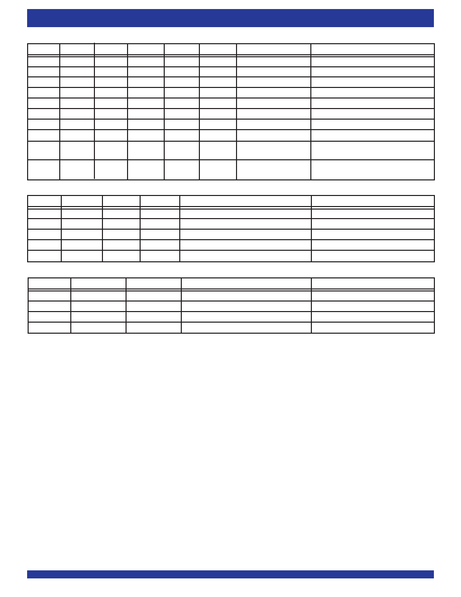
COMMERCIALTEMPERATURERANGE
IDT72V3656/72V3666/72V3676 3.3V CMOS TRIPLE BUS SyncFIFOTM
WITH BUS MATCHING 2,048 x 36 x 2, 4,096 x 36 x 2 and 8,192 x 36 x 2
CSA
W/
RA
ENA
MBA
CLKA
LOOP
Data A(A0-A35) I/O
PORT FUNCTION
H
X
H
High-Impedance
None
L
H
L
X
H
Input
None
LH
H
L
↑
H
Input
FIFO1 write
LH
H
↑
H
Input
Mail1 write
L
X
H
Output
None
LL
H
L
↑
H
Output
FIFO2 read
L
H
X
H
Output
None
LL
H
↑
H
Output
Mail2 read (set
MBF2 HIGH)
LH
H
L
↑
L
Output
Loop the data output of FIFO2 to input
of FIFO1 only
LL
H
L
↑
L
Output
Loop the data output of FIFO2 to input
of FIFO1 and put data on Port A
CSB
RENB
MBB
CLKB
Data B (B0-B17) Outputs
PORT FUNCTION
H
X
High-Impedance
None
L
X
Output
None
LH
L
↑
Output
FIFO1 read
L
H
X
Output
None
LH
H
↑
Output
Mail1 read (set
MBF1 HIGH)
TABLE 4
PORT C ENABLE FUNCTION TABLE
TABLE 3
PORT B ENABLE FUNCTION TABLE
WENC
MBC
CLKC
Data C (C0-C17) Inputs
PORT FUNCTION
HL
↑
Input
FIFO2 write
HH
↑
Input
Mail2 write
L
X
Input
None
L
H
X
Input
None
INTERSPERSED PARITY
Interspersed Parity is selected during a Master Reset of the FIFO. Refer to
Table 1 for the set-up configuration of Interspersed Parity. The Interspersed
Parity function allows the user to select the location of the parity bits in the word
loaded into the parallel port (A0-An) during programming of the flag offset
values. If Interspersed Parity is selected then during parallel programming of
the flag offset values, the device will ignore data line A8. If Non-Interspersed
ParityisselectedthendatalineA8willbecomeavalidbit.IfInterspersedParity
isselectedserialprogrammingoftheoffsetvaluesisnotpermitted,onlyparallel
programming can be done.
— SERIAL LOAD
ToprogramtheX1,X2,Y1,andY2registersserially,initiateaMasterReset
with FS2 LOW, FS0/SD LOW and FS1/
SEN HIGH during the LOW-to-HIGH
transition of
MRS1andMRS2.Afterthisresetiscomplete,theXandYregister
values are loaded bit-wise through the FS0/SD input on each LOW-to-HIGH
transition of CLKA that the FS1/
SEN input is LOW. There are 44-, 48-, or 52-
bitwritesneededtocompletetheprogrammingfortheIDT72V3656,IDT7V3666,
or IDT72V3676, respectively. The four registers are written in the order Y1,
X1, Y2 and finally, X2. The first-bit write stores the most significant bit of the Y1
registerandthelast-bitwritestorestheleastsignificantbitoftheX2register.Each
register value can be programmed from 1 to 2,044 (IDT72V3656), 1 to 4,092
(IDT72V3666), or 1 to 8,188 (IDT72V3676).
When the option to program the Offset registers serially is chosen, the Port
AFull/InputReady(
FFA/IRA)flagremainsLOWuntilallregisterbitsarewritten.
FFA/IRAissetHIGHbytheLOW-to-HIGHtransitionofCLKAafterthelastbit
is loaded to allow normal FIFO1 operation. The Port B Full/Input Ready (
FFC/
IRC) flag also remains LOW throughout the serial programming process, until
allregisterbitsarewritten.
FFC/IRCissetHIGHbytheLOW-to-HIGHtransition
of CLKC after the last bit is loaded to allow normal FIFO2 operation.
See Figure 9 timing diagram, Serial Programming of the Almost-Full Flag
and Almost-Empty Flag Offset Values after Reset (IDT Standard and FWFT
Modes).
FIFO WRITE/READ OPERATION
The state of the Port A data (A0-A35) outputs is controlled by Port A Chip
Select (
CSA)andPortAWrite/ReadSelect(W/RA).TheA0-A35outputsare
in the high-impedance state when either
CSA or W/RA is HIGH. The A0-A35
outputs are active when both
CSA and W/RA are LOW.
Data is loaded into FIFO1 from the A0-A35 inputs on a LOW-to-HIGH
transition of CLKA when
CSA is LOW, W/RA is HIGH, ENA is HIGH, MBA is
LOW, and
FFA/IRA is HIGH. Data is read from FIFO2 to the A0-A35 outputs
by a LOW-to-HIGH transition of CLKA when
CSAisLOW,W/RAisLOW,ENA
is HIGH, MBA is LOW, and
EFA/ORA is HIGH (see Table 2). FIFO reads and
writes on Port A are independent of any concurrent Port B or Port C
operation.
TABLE 2
PORT A ENABLE FUNCTION TABLE
相关PDF资料 |
PDF描述 |
|---|---|
| IDT72V3674L10PF8 | IC FIFO 16384X36 10NS 128QFP |
| VI-B5D-IV-F4 | CONVERTER MOD DC/DC 85V 150W |
| VI-B5D-IV-F2 | CONVERTER MOD DC/DC 85V 150W |
| VI-B5D-IV-F1 | CONVERTER MOD DC/DC 85V 150W |
| V150B48M250BF | CONVERTER MOD DC/DC 48V 250W |
相关代理商/技术参数 |
参数描述 |
|---|---|
| IDT72V3676L15PF | 功能描述:IC FIFO 16384X36 15NS 128QFP RoHS:否 类别:集成电路 (IC) >> 逻辑 - FIFO 系列:72V 标准包装:15 系列:74F 功能:异步 存储容量:256(64 x 4) 数据速率:- 访问时间:- 电源电压:4.5 V ~ 5.5 V 工作温度:0°C ~ 70°C 安装类型:通孔 封装/外壳:24-DIP(0.300",7.62mm) 供应商设备封装:24-PDIP 包装:管件 其它名称:74F433 |
| IDT72V3676L15PF8 | 功能描述:IC FIFO 16384X36 15NS 128QFP RoHS:否 类别:集成电路 (IC) >> 逻辑 - FIFO 系列:72V 标准包装:15 系列:74F 功能:异步 存储容量:256(64 x 4) 数据速率:- 访问时间:- 电源电压:4.5 V ~ 5.5 V 工作温度:0°C ~ 70°C 安装类型:通孔 封装/外壳:24-DIP(0.300",7.62mm) 供应商设备封装:24-PDIP 包装:管件 其它名称:74F433 |
| IDT72V3680L10PF | 功能描述:IC FIFO SS 16384X36 10NS 128TQFP RoHS:否 类别:集成电路 (IC) >> 逻辑 - FIFO 系列:72V 标准包装:15 系列:74F 功能:异步 存储容量:256(64 x 4) 数据速率:- 访问时间:- 电源电压:4.5 V ~ 5.5 V 工作温度:0°C ~ 70°C 安装类型:通孔 封装/外壳:24-DIP(0.300",7.62mm) 供应商设备封装:24-PDIP 包装:管件 其它名称:74F433 |
| IDT72V3680L10PF8 | 功能描述:IC FIFO SS 16384X36 10NS 128TQFP RoHS:否 类别:集成电路 (IC) >> 逻辑 - FIFO 系列:72V 标准包装:15 系列:74F 功能:异步 存储容量:256(64 x 4) 数据速率:- 访问时间:- 电源电压:4.5 V ~ 5.5 V 工作温度:0°C ~ 70°C 安装类型:通孔 封装/外壳:24-DIP(0.300",7.62mm) 供应商设备封装:24-PDIP 包装:管件 其它名称:74F433 |
| IDT72V3680L10PFI | 制造商:Integrated Device Technology Inc 功能描述: |
发布紧急采购,3分钟左右您将得到回复。