- 您现在的位置:买卖IC网 > PDF目录9942 > IDT72V3676L10PF8 (IDT, Integrated Device Technology Inc)IC FIFO 16384X36 10NS 128QFP PDF资料下载
参数资料
| 型号: | IDT72V3676L10PF8 |
| 厂商: | IDT, Integrated Device Technology Inc |
| 文件页数: | 6/39页 |
| 文件大小: | 0K |
| 描述: | IC FIFO 16384X36 10NS 128QFP |
| 标准包装: | 1,000 |
| 系列: | 72V |
| 功能: | 异步 |
| 存储容量: | 576K(16K x 36) |
| 数据速率: | 100MHz |
| 访问时间: | 10ns |
| 电源电压: | 3.15 V ~ 3.45 V |
| 工作温度: | 0°C ~ 70°C |
| 安装类型: | 表面贴装 |
| 封装/外壳: | 128-LQFP |
| 供应商设备封装: | 128-TQFP(14x20) |
| 包装: | 带卷 (TR) |
| 其它名称: | 72V3676L10PF8 |
第1页第2页第3页第4页第5页当前第6页第7页第8页第9页第10页第11页第12页第13页第14页第15页第16页第17页第18页第19页第20页第21页第22页第23页第24页第25页第26页第27页第28页第29页第30页第31页第32页第33页第34页第35页第36页第37页第38页第39页
14
COMMERCIALTEMPERATURERANGE
IDT72V3656/72V3666/72V3676 3.3V CMOS TRIPLE BUS SyncFIFOTM
WITH BUS MATCHING 2,048 x 36 x 2, 4,096 x 36 x 2 and 8,192 x 36 x 2
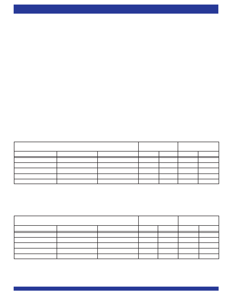
TABLE 5
FIFO1 FLAG OPERATION (IDT Standard and FWFT modes)
TABLE 6
FIFO2 FLAG OPERATION (IDT Standard and FWFT modes)
Synchronized
Number of Words in FIFO Memory(1,2)
to CLKB
to CLKA
IDT72V3656(3)
IDT72V3666(3)
IDT72V3676(3)
EFB/ORB
AEB
AFA
FFA/IRA
00
0
L
H
1 to X1
H
L
H
(X1+1) to [2,048-(Y1+1)]
(X1+1) to [4,096-(Y1+1)]
(X1+1) to [8,192-(Y1+1)]
H
(2,048-Y1) to 2,047
(4,096-Y1) to 4,095
(8,192-Y1) to 8,191
H
L
H
2,048
4,096
8,192
H
L
NOTES:
1. When a word loaded to an empty FIFO is shifted to the output register, its previous FIFO memory location is free.
2. Data in the output register does not count as a "word in FIFO memory". Since in FWFT mode, the first word written to an empty FIFO goes unrequested to the output register (no read operation
necessary), it is not included in the FIFO memory count.
3. X1 is the almost-empty offset for FIFO1 used by
AEB. Y1 is the almost-full offset for FIFO1 used by AFA. Both X1 and Y1 are selected during a FIFO1 reset or port A programming.
4. The ORB and IRA functions are active during FWFT mode; the
EFB and FFA functions are active in IDT Standard mode.
NOTES:
1. When a word loaded to an empty FIFO is shifted to the output register, its previous FIFO memory location is free.
2. Data in the output register does not count as a "word in FIFO memory". Since in FWFT mode, the first word written to an empty FIFO goes unrequested to the output register (no read operation
necessary), it is not included in the FIFO memory count.
3. X2 is the almost-empty offset for FIFO2 used by
AEA. Y2 is the almost-full offset for FIFO2 used by AFC. Both X2 and Y2 are selected during a FIFO2 reset or port A programming.
4. The ORA and IRC functions are active during FWFT mode; the
EFA and FFC functions are active in IDT Standard mode.
Synchronized
Number of Words in FIFO Memory
(1,2)
to CLKA
to CLKC
IDT72V3656(3)
IDT72V3666(3)
IDT72V3676(3)
EFA/ORA
AEA
AFC
FFC/IRC
00
0
L
H
1 to X2
H
L
H
(X2+1) to [2,048-(Y2+1)]
(X2+1) to [4,096-(Y2+1)]
(X2+1) to [8,192-(Y2+1)]
H
(2,048-Y2) to 2,047
(4,096-Y2) to 4,095
(8,192-Y2) to 8,191
H
L
H
2,048
4,096
8,192
H
L
The state of the Port B data (B0-B17) outputs is controlled by the Port B
Chip Select (
CSB). The B0-B17 outputs are in the high-impedance state
when
CSB is HIGH. The B0-B17 outputs are active when CSB is LOW.
Data is read from FIFO1 to the B0-B17 outputs by a LOW-to-HIGH
transition of CLKB when
CSBisLOW,RENBisHIGH,MBBisLOWandEFB/
ORB is HIGH (see Table 3). FIFO reads on Port B are independent of any
concurrent Port A and Port C operations.
Data is loaded into FIFO2 from the C0-C17 inputs on a LOW-to-HIGH
transition of CLKC when WENB is HIGH, MBC is LOW, and
FFC/IRCisHIGH
(see Table 4). FIFO writes on Port C are independent of any concurrent Port
A and Port B operation.
Thesetupandholdtimeconstraintsfor
CSAandW/RAwithregardtoCLKA
as well as
CSB with regard to CLKB are only for enabling write and read
operations and are not related to high-impedance control of the data outputs.
If ENA is LOW during a clock cycle, either
CSA or W/RA may change states
during the setup and hold time window of the cycle. This is also true for
CSB
when RENB is LOW.
WhenoperatingtheFIFOinFWFTmodeandtheOutputReadyflagisLOW,
the next word written is automatically sent to the FIFO’s output register by the
LOW-to-HIGHtransitionoftheportclockthatsetstheOutputReadyflagHIGH.
When the Output Ready flag is HIGH, subsequent data is clocked to the output
registersonlywhenareadisselectedusing
CSA,W/RA,ENAandMBAatPort
A or using
CSB, RENB and MBB at Port B.
When operating the FIFO in IDT Standard mode, the first word will cause
the Empty Flag to change state on the second LOW-to-HIGH transition of the
Read Clock. The data word will not be automatically sent to the output register.
Instead, data residing in the FIFO’s memory array is clocked to the output
register only when a read is selected using
CSA,W/RA,ENAandMBAatPort
A or using
CSB, RENB and MBB at Port B. Relevant write and read timing
diagrams for Port A can be found in Figure 10 and 15. Relevant read and write
timing diagrams for Port B and Port C, together with Bus-Matching and Endian
select operation, can be found in Figure 11 to 14.
LOOPBACK (
LOOP)
A Loopback function is provided on Port A and is selected by setting the
LOOPpinLOW.WhentheLoopfeatureisselected,thedataoutputfromFIFO2
will be directed to the data input of FIFO1. If Loop is selected and Port A is set-
upforwriteoperationviatheW/RApinbeingHIGH,thendataoutputfromFIFO2
will be written to FIFO1, on every LOW-to-HIGH transition of CLKA, provided
CSAisLOWandENAisHIGH.However,FIFO2dataoutputwillnotbeplaced
on the output Port A (A0-A35). If Port A is set-up for read operation via the W/
RA pin being LOW, then data output from FIFO2 will be written into FIFO1 on
every LOW-to-HIGH transition of CLKA, provided
CSA is LOW and ENA is
HIGH. Also FIFO2 data will be output to Port A (A0-A35). When the
LOOP
pin is HIGH then Port A operates in the normal manner. Refer to Table 2 for
the input set-up of the Loop feature.
The Loop operation will continue to happen provided that FIFO1 is not full
and FIFO2 is not empty. If during a Loop sequence FIFO1 becomes full then
any data that continues to be read out from FIFO2 will only be placed on the
Port A (A0-A35) lines, (provided that Port A is set-up for read operation). If
相关PDF资料 |
PDF描述 |
|---|---|
| IDT72V3674L10PF8 | IC FIFO 16384X36 10NS 128QFP |
| VI-B5D-IV-F4 | CONVERTER MOD DC/DC 85V 150W |
| VI-B5D-IV-F2 | CONVERTER MOD DC/DC 85V 150W |
| VI-B5D-IV-F1 | CONVERTER MOD DC/DC 85V 150W |
| V150B48M250BF | CONVERTER MOD DC/DC 48V 250W |
相关代理商/技术参数 |
参数描述 |
|---|---|
| IDT72V3676L15PF | 功能描述:IC FIFO 16384X36 15NS 128QFP RoHS:否 类别:集成电路 (IC) >> 逻辑 - FIFO 系列:72V 标准包装:15 系列:74F 功能:异步 存储容量:256(64 x 4) 数据速率:- 访问时间:- 电源电压:4.5 V ~ 5.5 V 工作温度:0°C ~ 70°C 安装类型:通孔 封装/外壳:24-DIP(0.300",7.62mm) 供应商设备封装:24-PDIP 包装:管件 其它名称:74F433 |
| IDT72V3676L15PF8 | 功能描述:IC FIFO 16384X36 15NS 128QFP RoHS:否 类别:集成电路 (IC) >> 逻辑 - FIFO 系列:72V 标准包装:15 系列:74F 功能:异步 存储容量:256(64 x 4) 数据速率:- 访问时间:- 电源电压:4.5 V ~ 5.5 V 工作温度:0°C ~ 70°C 安装类型:通孔 封装/外壳:24-DIP(0.300",7.62mm) 供应商设备封装:24-PDIP 包装:管件 其它名称:74F433 |
| IDT72V3680L10PF | 功能描述:IC FIFO SS 16384X36 10NS 128TQFP RoHS:否 类别:集成电路 (IC) >> 逻辑 - FIFO 系列:72V 标准包装:15 系列:74F 功能:异步 存储容量:256(64 x 4) 数据速率:- 访问时间:- 电源电压:4.5 V ~ 5.5 V 工作温度:0°C ~ 70°C 安装类型:通孔 封装/外壳:24-DIP(0.300",7.62mm) 供应商设备封装:24-PDIP 包装:管件 其它名称:74F433 |
| IDT72V3680L10PF8 | 功能描述:IC FIFO SS 16384X36 10NS 128TQFP RoHS:否 类别:集成电路 (IC) >> 逻辑 - FIFO 系列:72V 标准包装:15 系列:74F 功能:异步 存储容量:256(64 x 4) 数据速率:- 访问时间:- 电源电压:4.5 V ~ 5.5 V 工作温度:0°C ~ 70°C 安装类型:通孔 封装/外壳:24-DIP(0.300",7.62mm) 供应商设备封装:24-PDIP 包装:管件 其它名称:74F433 |
| IDT72V3680L10PFI | 制造商:Integrated Device Technology Inc 功能描述: |
发布紧急采购,3分钟左右您将得到回复。