- 您现在的位置:买卖IC网 > Datasheet目录332 > IR22141SSPBF (International Rectifier)IC DRIVER HALF BRIDGE SGL 24SSOP Datasheet资料下载
参数资料
| 型号: | IR22141SSPBF |
| 厂商: | International Rectifier |
| 文件页数: | 12/34页 |
| 文件大小: | 0K |
| 描述: | IC DRIVER HALF BRIDGE SGL 24SSOP |
| 标准包装: | 55 |
| 配置: | 半桥 |
| 输入类型: | 非反相 |
| 延迟时间: | 440ns |
| 电流 - 峰: | 2A |
| 配置数: | 1 |
| 输出数: | 2 |
| 高端电压 - 最大(自引导启动): | 1200V |
| 电源电压: | 11.5 V ~ 20 V |
| 工作温度: | -40°C ~ 125°C |
| 安装类型: | 表面贴装 |
| 封装/外壳: | 24-SSOP(0.209",5.30mm 宽) |
| 供应商设备封装: | 24-SSOP |
| 包装: | 管件 |
| 配用: | IRMD2214SS-ND - KIT DESIGN EVAL BOARD IR2214SS IRMD22141SS-ND - KIT DESIGN EVAL BOARD/IR22141SS |
第1页第2页第3页第4页第5页第6页第7页第8页第9页第10页第11页当前第12页第13页第14页第15页第16页第17页第18页第19页第20页第21页第22页第23页第24页第25页第26页第27页第28页第29页第30页第31页第32页第33页第34页
�� �
�
�IR21141/IR22141SSPbF�
�1.4� Fault� Management�
�1 Features Description�
�1.1� Start-Up� Sequence�
�At� power� supply� start-up,� it� is� recommended� to� keep� the�
�FLT_CLR� pin� active� until� the� supply� voltages� are�
�properly� established.� This� prevents� spurious� diagnostic�
�signals� being� generated.�
�When� the� bootstrap� supply� topology� is� used� for�
�supplying� the� floating� high� side� stage,� the� following� start-�
�The� IR21141/IR22141� is� able� to� manage� supply� failure�
�(undervoltage� lockout)� and� transistor� desaturation� (on�
�both� the� low� and� high� side� switches).�
�1.4.1� Undervoltage� (UV)�
�The� undervoltage� protection� function� disables� the�
�driver’s� output� stage� which� prevents� the� power� device�
�from� being� driven� when� the� input� voltage� is� less� than� the�
�undervoltage� threshold.� Both� the� low� side� (V� CC� supplied)�
�and� the� floating� side� (V� BS� supplied)� are� controlled� by� a�
�dedicate� undervoltage� function.�
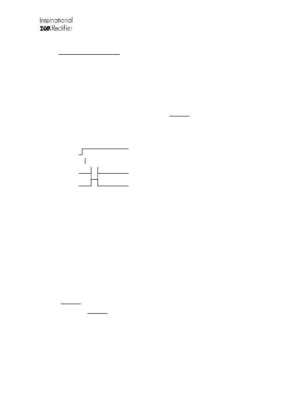
�up� sequence� is� recommended� (see� also� Fig.� 12):�
�An� undervoltage� event� on� the� V� CC�
�pin� (when�
�1.�
�2.�
�3.�
�4.�
�5.�
�Set� V� CC� ,�
�Set� FLT_CLR� pin� to� HIGH� level,�
�Set� LIN� pin� to� HIGH� level� and� charge� the�
�bootstrap� capacitor,�
�Release� LIN� pin� to� LOW� level,�
�Release� FLT_CLR� pin� to� LOW� level.�
�VCC�
�FLT_CLR�
�LIN�
�LO�
�V� CC� < UV� VCC-� )� generates� a� diagnostic� signal� by� forcing�
�the� FAULT/SD� pin� low� (see� FAULT/SD� section� and� Fig.�
�14).� This� event� disables� both� the� low� side� and� floating�
�drivers� and� the� diagnostic� signal� holds� until� the�
�undervoltage� condition� is� over.� The� fault� condition� is� not�
�latched� and� the� FAULT/SD� pin� is� released� once� V� CC�
�becomes� higher� than� UV� VCC+� .�
�The� V� BS� undervoltage� protection� works� by� disabling� only�
�the� floating� driver.� Undervoltage� on� V� BS� does� not� prevent�
�the� low� side� driver� from� activating� its� output� nor� does� it�
�generate� diagnostic� signals.� The� V� BS� undervoltage�
�condition� (V� BS� <� UV� VBS-� )� latches� the� high� side� output�
�stage� in� the� low� state.� V� BS� must� exceed� the� UV� VBS+�
�threshold� to� return� the� device� to� its� normal� operating�
�mode.� To� turn� on� the� floating� driver,� H� IN� must� be� re-�
�Figure� 12� Start-Up� Sequence�
�A� minimum� 15� μs� LIN� and� FLT-CLR� pulse� is� required.�
�A� minimum� supply� voltage� of� 8V� is� recommended� for� the�
�driver� to� operate� safely� under� switching� conditions� at� VS�
�pin.� At� lower� supply� the� gate� driving� capability� decreases�
�and� might� become� not� sufficient� to� counteract� switching�
�charge� injected� to� the� outputs.�
�1.2� Normal� Operation� Mode�
�After� the� start-up� sequence� has� completed,� the� device�
�becomes� fully� operative� (see� grey� blocks� in� the� State�
�Diagram).�
�HIN� and� LIN� produce� driver� outputs� to� switch�
�accordingly,� while� the� input� logic� monitors� the� input�
�signals� and� deadtime� (DT)� prevent� shoot-through� events�
�from� occurring.�
�1.3� Shutdown�
�The� system� controller� can� asynchronously� command� the�
�Hard� Shutdown� (HSD)� through� the� 3.3� V� compatible�
�CMOS� I/O� FAULT/SD� pin.� This� event� is� not� latched.�
�In� a� multi-phase� system,� FAULT/SD� signals� are� or-ed� so�
�the� controller� or� one� of� the� gate� drivers� can� force� the�
�simultaneous� shutdown� of� the� other� gate� drivers� through�
�the� same� pin.�
�www.irf.com�
�12�
�asserted� high� (rising� edge� event� on� H� IN� is� required).�
�1.4.2� Power� Devices� Desaturation�
�Different� causes� can� generate� a� power� inverter� failure�
�(phase� and/or� rail� supply� short-circuit,� overload�
�conditions� induced� by� the� load,� etc.).� In� all� of� these� fault�
�conditions,� a� large� increase� in� current� results� in� the�
�IGBT.�
�The� IR21141/IR22141� fault� detection� circuit� monitors� the�
�IGBT� emitter� to� collector� voltage� (V� CE� )� (an� external� high�
�voltage� diode� is� connected� between� the� IGBT’s� collector�
�and� the� ICs� DSH� or� DSL� pins).� A� high� current� in� the�
�IGBT� may� cause� the� transistor� to� desaturate;� this�
�condition� results� in� an� increase� of� V� CE� .�
�Once� in� desaturation,� the� current� in� the� power� transistor�
�can� be� as� high� as� 10� times� the� nominal� current.�
�Whenever� the� transistor� is� switched� off,� this� high� current�
�generates� relevant� voltage� transients� in� the� power� stage�
�that� need� to� be� smoothed� out� in� order� to� avoid�
�destruction� (by� over-voltage).� The� gate� driver� is� able� to�
�control� the� transient� condition� by� smoothly� turning� off� the�
�desaturated� transistor� with� its� integrated� soft� shutdown�
�(SSD)� protection.�
�1.4.3� Desaturation� Detection:� DSH/L� Function�
�Figure� 13� shows� the� structure� of� the� desaturation�
�sensing� and� soft� shutdown� block.� This� configuration� is�
�the� same� for� both� the� high� and� low� side� output� stages.�
�?� 2009� International� Rectifier�
�相关PDF资料 |
PDF描述 |
|---|---|
| IR2235JPBF | IC DRIVER BRIDGE 3PHASE 44PLCC |
| IR2301PBF | IC DRIVER HIGH/LOW SIDE 8DIP |
| IR2302PBF | IC DRIVER HALF BRIDGE 8DIP |
| IR2304SPBF | IC DRIVER HALF BRIDGE 8-SOIC |
| IR2308SPBF | IC DRIVER HALF BRIDGE HV 8SOIC |
相关代理商/技术参数 |
参数描述 |
|---|---|
| IR22141SSPBF | 制造商:International Rectifier 功能描述:Driver IC |
| IR22141SSTRPBF | 功能描述:功率驱动器IC Hlf Brdg Drvr IC for Pwr Swtch App RoHS:否 制造商:Micrel 产品:MOSFET Gate Drivers 类型:Low Cost High or Low Side MOSFET Driver 上升时间: 下降时间: 电源电压-最大:30 V 电源电压-最小:2.75 V 电源电流: 最大功率耗散: 最大工作温度:+ 85 C 安装风格:SMD/SMT 封装 / 箱体:SOIC-8 封装:Tube |
| IR2214SS | 功能描述:IC DRIVER HALF BRIDGE SGL 24SSOP RoHS:否 类别:集成电路 (IC) >> PMIC - MOSFET,电桥驱动器 - 外部开关 系列:- 标准包装:50 系列:- 配置:高端 输入类型:非反相 延迟时间:200ns 电流 - 峰:250mA 配置数:1 输出数:1 高端电压 - 最大(自引导启动):600V 电源电压:12 V ~ 20 V 工作温度:-40°C ~ 125°C 安装类型:通孔 封装/外壳:8-DIP(0.300",7.62mm) 供应商设备封装:8-DIP 包装:管件 其它名称:*IR2127 |
| IR2214SSPBF | 功能描述:功率驱动器IC 1200V HALF BRDG DRVR IC RoHS:否 制造商:Micrel 产品:MOSFET Gate Drivers 类型:Low Cost High or Low Side MOSFET Driver 上升时间: 下降时间: 电源电压-最大:30 V 电源电压-最小:2.75 V 电源电流: 最大功率耗散: 最大工作温度:+ 85 C 安装风格:SMD/SMT 封装 / 箱体:SOIC-8 封装:Tube |
| IR2214SSPBF | 制造商:International Rectifier 功能描述:Driver IC |
发布紧急采购,3分钟左右您将得到回复。