- 您现在的位置:买卖IC网 > PDF目录377504 > IRF5210S (International Rectifier) Power MOSFET(Vdss=-100V, Rds(on)=0.06ohm, Id=-40A) PDF资料下载
参数资料
| 型号: | IRF5210S |
| 厂商: | International Rectifier |
| 英文描述: | Power MOSFET(Vdss=-100V, Rds(on)=0.06ohm, Id=-40A) |
| 中文描述: | 功率MOSFET(减振钢板基本\u003d- 100V的,的Rds(on)\u003d 0.06ohm,身份证\u003d- 40A条) |
| 文件页数: | 2/10页 |
| 文件大小: | 186K |
| 代理商: | IRF5210S |
IRF5210S/L
Starting T
J
= 25°C, L = 3.1mH
R
G
= 25
, I
AS
= -21A. (See Figure 12)
I
SD
≤
-21A, di/dt
≤
-480A/μs, V
DD
≤
V
(BR)DSS
,
T
J
≤
175°C
Repetitive rating; pulse width limited by
max. junction temperature. ( See fig. 11 )
Notes:
** When mounted on 1" square PCB (FR-4 or G-10 Material ).
For recommended footprint and soldering techniques refer to application note #AN-994.
Pulse width
≤
300μs; duty cycle
≤
2%.
Uses IRF5210 data and test conditions
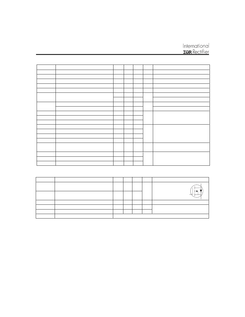
Source-Drain Ratings and Characteristics
Parameter
I
S
Continuous Source Current
(Body Diode)
I
SM
Pulsed Source Current
(Body Diode)
V
SD
Diode Forward Voltage
t
rr
Reverse Recovery Time
Q
rr
Reverse Recovery Charge
t
on
Forward Turn-On Time
Parameter
Min. Typ. Max. Units
-100
–––
–––
-0.11 –––
–––
–––
-2.0
–––
10
–––
–––
–––
–––
–––
–––
–––
–––
–––
–––
–––
–––
–––
–––
–––
–––
17
–––
86
–––
79
–––
81
Conditions
V
GS
= 0V, I
D
= -250μA
Reference to 25°C, I
D
= -1mA
V
GS
= -10V, I
D
= -24A
V
DS
= V
GS
, I
D
= -250μA
V
DS
= -50V, I
D
= -21A
V
DS
= -100V, V
GS
= 0V
V
DS
= -80V, V
GS
= 0V, T
J
= 150°C
V
GS
= 20V
V
GS
= -20V
I
D
= -21A
V
DS
= -80V
V
GS
= -10V, See Fig. 6 and 13
V
DD
= -50V
I
D
= -21A
R
G
= 2.5
R
D
= 2.4
,
See Fig. 10
Between lead,
and center of die contact
V
GS
= 0V
V
DS
= -25V
= 1.0MHz, See Fig. 5
V
(BR)DSS
V
(BR)DSS
/
T
J
Breakdown Voltage Temp. Coefficient
R
DS(on)
Static Drain-to-Source On-Resistance
V
GS(th)
Gate Threshold Voltage
g
fs
Forward Transconductance
Drain-to-Source Breakdown Voltage
–––
V
V/°C
V
S
0.06
-4.0
–––
-25
-250
100
-100
180
25
97
–––
–––
–––
–––
μA
Gate-to-Source Forward Leakage
Gate-to-Source Reverse Leakage
Total Gate Charge
Gate-to-Source Charge
Gate-to-Drain ("Miller") Charge
Turn-On Delay Time
Rise Time
Turn-Off Delay Time
Fall Time
nA
Q
g
Q
gs
Q
gd
t
d(on)
t
r
t
d(off)
t
f
nC
–––
–––
C
iss
C
oss
C
rss
Input Capacitance
Output Capacitance
Reverse Transfer Capacitance
–––
–––
–––
2700 –––
790
450
–––
–––
pF
Electrical Characteristics @ T
J
= 25°C (unless otherwise specified)
I
GSS
ns
I
DSS
Drain-to-Source Leakage Current
nH
7.5
L
S
Internal Source Inductance
Min. Typ. Max. Units
Conditions
MOSFET symbol
showing the
integral reverse
p-n junction diode.
T
J
= 25°C, I
S
= -24A, V
GS
= 0V
T
J
= 25°C, I
F
= -21A
di/dt = -100A/μs
–––
–––
–––
–––
–––
–––
–––
–––
170
1.2
-1.6
260
1.8
V
ns
μC
Intrinsic turn-on time is negligible (turn-on is dominated by L
S
+L
D
)
A
S
D
G
-40
-140
相关PDF资料 |
PDF描述 |
|---|---|
| IRF5210 | Power MOSFET(Vdss=-100V, Rds(on)=0.06ohm, Id=-40A) |
| IRF5305PBF | HEXFET Power MOSFET |
| IRF5305 | Power MOSFET(Vdss=-55V, Rds(on)=0.06ohm, Id=-31A) |
| IRF530L | Power MOSFET(Vdss=100V, Rds(on)=0.11ohm, Id=17A) |
| IRF530FI | N - CHANNEL ENHANCEMENT MODE POWER MOS TRANSISTOR |
相关代理商/技术参数 |
参数描述 |
|---|---|
| IRF5210SHR | 制造商:International Rectifier 功能描述:Trans MOSFET P-CH 100V 40A 3-Pin(2+Tab) D2PAK 制造商:International Rectifier 功能描述:TRANS MOSFET P-CH 100V 40A 3PIN D2PAK - Rail/Tube |
| IRF5210SPBF | 功能描述:MOSFET 1 P-CH -100V HEXFET 60mOhms 120nC RoHS:否 制造商:STMicroelectronics 晶体管极性:N-Channel 汲极/源极击穿电压:650 V 闸/源击穿电压:25 V 漏极连续电流:130 A 电阻汲极/源极 RDS(导通):0.014 Ohms 配置:Single 最大工作温度: 安装风格:Through Hole 封装 / 箱体:Max247 封装:Tube |
| IRF5210STRL | 制造商:International Rectifier 功能描述:MOSFET Transistor, P-Channel, TO-263AB |
| IRF5210STRLHR | 制造商:International Rectifier 功能描述:Trans MOSFET P-CH 100V 40A 3-Pin(2+Tab) D2PAK T/R 制造商:International Rectifier 功能描述:TRANS MOSFET P-CH 100V 40A 3PIN D2PAK - Tape and Reel |
| IRF5210STRLPBF | 功能描述:MOSFET MOSFT PCh -100V -0.4A 60mOhm 120nC RoHS:否 制造商:STMicroelectronics 晶体管极性:N-Channel 汲极/源极击穿电压:650 V 闸/源击穿电压:25 V 漏极连续电流:130 A 电阻汲极/源极 RDS(导通):0.014 Ohms 配置:Single 最大工作温度: 安装风格:Through Hole 封装 / 箱体:Max247 封装:Tube |
发布紧急采购,3分钟左右您将得到回复。