- 您现在的位置:买卖IC网 > PDF目录18347 > IRFU1010ZPBF (International Rectifier)MOSFET N-CH 55V 42A I-PAK PDF资料下载
参数资料
| 型号: | IRFU1010ZPBF |
| 厂商: | International Rectifier |
| 文件页数: | 2/11页 |
| 文件大小: | 0K |
| 描述: | MOSFET N-CH 55V 42A I-PAK |
| 标准包装: | 75 |
| 系列: | HEXFET® |
| FET 型: | MOSFET N 通道,金属氧化物 |
| FET 特点: | 标准 |
| 漏极至源极电压(Vdss): | 55V |
| 电流 - 连续漏极(Id) @ 25° C: | 42A |
| 开态Rds(最大)@ Id, Vgs @ 25° C: | 7.5 毫欧 @ 42A,10V |
| Id 时的 Vgs(th)(最大): | 4V @ 100µA |
| 闸电荷(Qg) @ Vgs: | 95nC @ 10V |
| 输入电容 (Ciss) @ Vds: | 2840pF @ 25V |
| 功率 - 最大: | 140W |
| 安装类型: | 通孔 |
| 封装/外壳: | TO-251-3 长引线,IPak,TO-251AB |
| 供应商设备封装: | I-Pak |
| 包装: | 管件 |
| 其它名称: | *IRFU1010ZPBF |
�� �
�
�IRFR/U1010ZPbF�
�Electrical� Characteristics� @� T� J� =� 25°C� (unless� otherwise� specified)�
�Parameter�
�Min.� Typ.� Max.� Units�
�Conditions�
�V� (BR)DSS�
�Drain-to-Source� Breakdown� Voltage�
�55�
�–––�
�–––�
�V�
�V� GS� =� 0V,� I� D� =� 250μA�
�?� V� (BR)DSS� /� ?� T� J�
�R� DS(on)�
�Breakdown� Voltage� Temp.� Coefficient�
�Static� Drain-to-Source� On-Resistance�
�–––�
�–––�
�0.051�
�5.8�
�–––�
�7.5�
�V/°C� Reference� to� 25°C,� I� D� =� 1mA�
�m� ?� V� GS� =� 10V,� I� D� =� 42A�
�V� GS(th)�
�gfs�
�I� DSS�
�Gate� Threshold� Voltage�
�Forward� Transconductance�
�Drain-to-Source� Leakage� Current�
�2.0�
�31�
�–––�
�–––�
�–––�
�–––�
�4.0�
�–––�
�20�
�V�
�S�
�μA�
�V� DS� =� V� GS� ,� I� D� =� 100μA�
�V� DS� =� 25V,� I� D� =� 42A�
�V� DS� =� 55V,� V� GS� =� 0V�
�–––�
�–––�
�250�
�V� DS� =� 55V,� V� GS� =� 0V,� T� J� =� 125°C�
�I� GSS�
�Q� g�
�Q� gs�
�Q� gd�
�t� d(on)�
�t� r�
�t� d(off)�
�t� f�
�Gate-to-Source� Forward� Leakage�
�Gate-to-Source� Reverse� Leakage�
�Total� Gate� Charge�
�Gate-to-Source� Charge�
�Gate-to-Drain� ("Miller")� Charge�
�Turn-On� Delay� Time�
�Rise� Time�
�Turn-Off� Delay� Time�
�Fall� Time�
�–––�
�–––�
�–––�
�–––�
�–––�
�–––�
�–––�
�–––�
�–––�
�–––�
�–––�
�63�
�17�
�23�
�17�
�76�
�42�
�48�
�200�
�-200�
�95�
�–––�
�–––�
�–––�
�–––�
�–––�
�–––�
�nA�
�nC�
�ns�
�V� GS� =� 20V�
�V� GS� =� -20V�
�I� D� =� 42A�
�V� DS� =� 44V�
�V� GS� =� 10V�
�V� DD� =� 28V�
�I� D� =� 42A�
�R� G� =� 7.6� ?�
�V� GS� =� 10V�
�L� D�
�Internal� Drain� Inductance�
�–––�
�4.5�
�–––�
�Between� lead,�
�D�
�L� S�
�Internal� Source� Inductance�
�–––�
�7.5�
�–––�
�nH�
�6mm� (0.25in.)�
�from� package�
�G�
�and� center� of� die� contact�
�S�
�C� iss�
�C� oss�
�Input� Capacitance�
�Output� Capacitance�
�–––�
�–––�
�2840�
�470�
�–––�
�–––�
�V� GS� =� 0V�
�V� DS� =� 25V�
�C� rss�
�C� oss�
�C� oss�
�C� oss� eff.�
�Reverse� Transfer� Capacitance�
�Output� Capacitance�
�Output� Capacitance�
�Effective� Output� Capacitance�
�–––�
�–––�
�–––�
�–––�
�250�
�1630�
�360�
�560�
�–––�
�–––�
�–––�
�–––�
�pF�
�?� =� 1.0MHz�
�V� GS� = 0V, V� DS� = 1.0V, ? = 1.0MHz�
�V� GS� = 0V, V� DS� = 44V, ? = 1.0MHz�
�V� GS� =� 0V,� V� DS� =� 0V� to� 44V�
�Source-Drain� Ratings� and� Characteristics�
�Parameter�
�Min.� Typ.� Max.� Units�
�Conditions�
�I� S�
�Continuous� Source� Current�
�–––�
�–––�
�42�
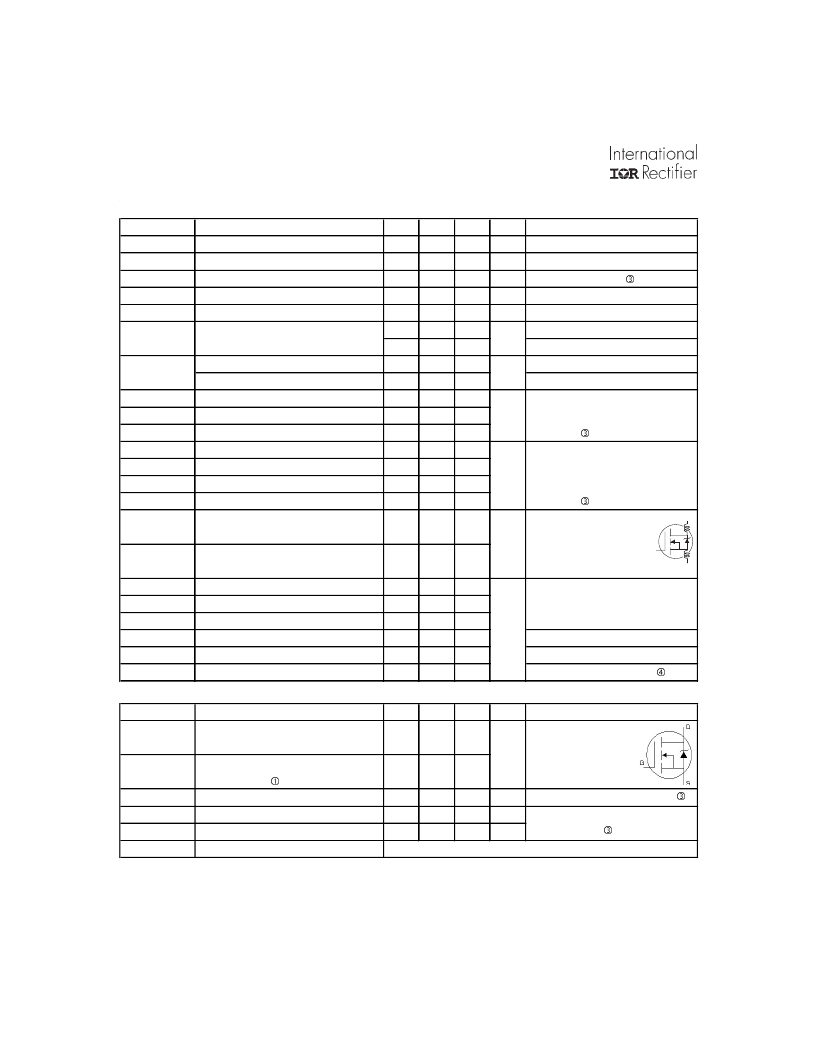
�MOSFET� symbol�
�(Body� Diode)�
�A�
�showing� the�
�I� SM�
�Pulsed� Source� Current�
�–––�
�–––�
�360�
�integral� reverse�
�(Body� Diode)�
�p-n� junction� diode.�
�V� SD�
�t� rr�
�Q� rr�
�Diode� Forward� Voltage�
�Reverse� Recovery� Time�
�Reverse� Recovery� Charge�
�–––�
�–––�
�–––�
�–––�
�24�
�20�
�1.3�
�36�
�30�
�V�
�ns�
�nC�
�T� J� =� 25°C,� I� S� =� 42A,� V� GS� =� 0V�
�T� J� =� 25°C,� I� F� =� 42A,� V� DD� =� 28V�
�di/dt� =� 100A/μs�
�t� on�
�2�
�Forward� Turn-On� Time�
�Intrinsic� turn-on� time� is� negligible� (turn-on� is� dominated� by� LS+LD)�
�www.irf.com�
�相关PDF资料 |
PDF描述 |
|---|---|
| M2012TXW13-DA | SWITCH ROCKER SPDT 6A 125V |
| M2012TYW01-JC | SWITCH ROCKER SPDT 6A 125V |
| M2012TYW01-JB | SWITCH ROCKER SPDT 6A 125V |
| M2013TJW02 | SWITCH ROCKER SPDT 6A 125V |
| M2012TXG13/108 | SWITCH ROCKER SPDT 0.4VA 28V |
相关代理商/技术参数 |
参数描述 |
|---|---|
| IRFU1018EPBF | 功能描述:MOSFET MOSFT 60V 79A 8.4mOhm 46nC Qg RoHS:否 制造商:STMicroelectronics 晶体管极性:N-Channel 汲极/源极击穿电压:650 V 闸/源击穿电压:25 V 漏极连续电流:130 A 电阻汲极/源极 RDS(导通):0.014 Ohms 配置:Single 最大工作温度: 安装风格:Through Hole 封装 / 箱体:Max247 封装:Tube |
| IRFU110 | 功能描述:MOSFET N-Chan 100V 4.3 Amp RoHS:否 制造商:STMicroelectronics 晶体管极性:N-Channel 汲极/源极击穿电压:650 V 闸/源击穿电压:25 V 漏极连续电流:130 A 电阻汲极/源极 RDS(导通):0.014 Ohms 配置:Single 最大工作温度: 安装风格:Through Hole 封装 / 箱体:Max247 封装:Tube |
| IRFU110_R4941 | 功能描述:MOSFET TO-251AA RoHS:否 制造商:STMicroelectronics 晶体管极性:N-Channel 汲极/源极击穿电压:650 V 闸/源击穿电压:25 V 漏极连续电流:130 A 电阻汲极/源极 RDS(导通):0.014 Ohms 配置:Single 最大工作温度: 安装风格:Through Hole 封装 / 箱体:Max247 封装:Tube |
| IRFU110A | 制造商:FAIRCHILD 制造商全称:Fairchild Semiconductor 功能描述:Advanced Power MOSFET |
| IRFU110ATU | 功能描述:MOSFET 100V Single RoHS:否 制造商:STMicroelectronics 晶体管极性:N-Channel 汲极/源极击穿电压:650 V 闸/源击穿电压:25 V 漏极连续电流:130 A 电阻汲极/源极 RDS(导通):0.014 Ohms 配置:Single 最大工作温度: 安装风格:Through Hole 封装 / 箱体:Max247 封装:Tube |
发布紧急采购,3分钟左右您将得到回复。