- 您现在的位置:买卖IC网 > PDF目录20668 > ISL6236EVAL2 (Intersil)EVAL BOARD 2 FOR ISL6236 PDF资料下载
参数资料
| 型号: | ISL6236EVAL2 |
| 厂商: | Intersil |
| 文件页数: | 7/35页 |
| 文件大小: | 0K |
| 描述: | EVAL BOARD 2 FOR ISL6236 |
| 标准包装: | 1 |
| 系列: | * |
第1页第2页第3页第4页第5页第6页当前第7页第8页第9页第10页第11页第12页第13页第14页第15页第16页第17页第18页第19页第20页第21页第22页第23页第24页第25页第26页第27页第28页第29页第30页第31页第32页第33页第34页第35页
�� �
�
�ISL6236�
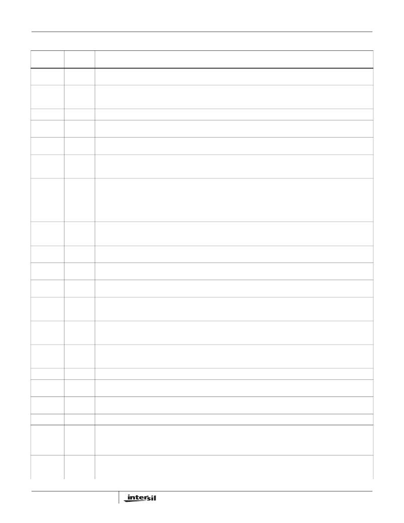
�Pin� Descriptions�
�PIN�
�NUMBER�
�1�
�2�
�3�
�4�
�5�
�6�
�7�
�NAME�
�REF�
�TON�
�VCC�
�EN� LDO�
�VREF3�
�VIN�
�LDO�
�FUNCTION�
�2V� Reference� Output.� Bypass� to� GND� with� a� 0.1μF� (min)� capacitor.� REF� can� source� up� to� 50μA� for� external� loads.�
�Loading� REF� degrades� FB� and� output� accuracy� according� to� the� REF� load-regulation� error.�
�Frequency� Select� Input.� Connect� to� GND� for� 400kHz/500kHz� operation.� Connect� to� REF� (or� leave� OPEN)� for�
�400kHz/300kHz� operation.� Connect� to� VCC� for� 200kHz/300kHz� operation� (5V/3.3V� SMPS� switching� frequencies,�
�respectively.)�
�Analog� Supply� Voltage� Input� for� PWM� Core.� Bypass� to� GND� with� a� 1μF� ceramic� capacitor.�
�LDO� Enable� Input.� The� LDO� is� enabled� if� EN� LDO� is� within� logic� high� level� and� disabled� if� EN� LDO� is� less� than� the� logic�
�low� level.�
�3.3V� Reference� Output.� VREF3� can� source� up� to� 5mA� for� external� loads.� Bypass� to� GND� with� a� 0.01μF� capacitor� if�
�loaded.� Leave� open� if� there� is� no� load.�
�Power-Supply� Input.� VIN� is� used� for� the� constant-on-time� PWM� on-time� one-shot� circuits.� VIN� is� also� used� to� power� the�
�linear� regulators.� The� linear� regulators� are� powered� by� SMPS1� if� OUT1� is� set� greater� than� 4.78V� and� BYP� is� tied� to�
�OUT1.� Connect� VIN� to� the� battery� input� and� bypass� with� a� 1μF� capacitor.�
�Linear-Regulator� Output.� LDO� can� provide� a� total� of� 100mA� external� loads.� The� LDO� regulate� at� 5V� If� LDOREFIN� is�
�connected� to� GND.� When� the� LDO� is� set� at� 5V� and� BYP� is� within� 5V� switchover� threshold,� the� internal� regulator� shuts�
�down� and� the� LDO� output� pin� connects� to� BYP� through� a� 0.7� Ω� switch.� The� LDO� regulate� at� 3.3V� if� LDOREFIN� is�
�connected� to� VCC.� When� the� LDO� is� set� at� 3.3V� and� BYP� is� within� 3.3V� switchover� threshold,� the� internal� regulator�
�shuts� down� and� the� LDO� output� pin� connects� to� BYP� through� a� 1.5� Ω� switch.� Bypass� LDO� output� with� a� minimum� of�
�4.7μF� ceramic.�
�8�
�LDOREFIN� LDO� Reference� Input.� Connect� LDOREFIN� to� GND� for� fixed� 5V� operation.� Connect� LDOREFIN� to� VCC� for� fixed� 3.3V�
�operation.� LDOREFIN� can� be� used� to� program� LDO� output� voltage� from� 0.7V� to� 4.5V.� LDO� output� is� two� times� the�
�voltage� of� LDOREFIN.� There� is� no� switchover� in� adjustable� mode.�
�9�
�10�
�11�
�12�
�13�
�14�
�15�
�16�
�17�
�18�
�19�
�20�
�BYP�
�OUT1�
�FB1�
�ILIM1�
�POK1�
�EN1�
�UGATE1�
�PHASE1�
�BOOT1�
�LGATE1�
�PVCC�
�SECFB�
�BYP� is� the� switchover� source� voltage� for� the� LDO� when� LDOREFIN� connected� to� GND� or� VCC.� Connect� BYP� to� 5V� if�
�LDOREFIN� is� tied� to� GND.� Connect� BYP� to� 3.3V� if� LDOREFIN� is� tied� to� VCC.�
�SMPS1� Output� Voltage-Sense� Input.� Connect� to� the� SMPS1� output.� OUT1� is� an� input� to� the� Constant� on-time-PWM�
�on-time� one-shot� circuit.� It� also� serves� as� the� SMPS1� feedback� input� in� fixed-voltage� mode.�
�SMPS1� Feedback� Input.� Connect� FB1� to� GND� for� fixed� 5V� operation.� Connect� FB1� to� VCC� for� fixed� 1.5V� operation�
�Connect� FB1� to� a� resistive� voltage-divider� from� OUT1� to� GND� to� adjust� the� output� from� 0.7V� to� 5.5V.�
�SMPS1� Current-Limit� Adjustment.� The� GND-PHASE1� current-limit� threshold� is� 1/10th� the� voltage� seen� at� ILIM1� over� a�
�0.2V� to� 2V� range.� There� is� an� internal� 5μA� current� source� from� VCC� to� ILIM1.� Connect� ILIM1� to� REF� for� a� fixed� 200mV�
�threshold.� The� logic� current� limit� threshold� is� default� to� 100mV� value� if� ILIM1� is� higher� than� VCC� -� 1V.�
�SMPS1� Power-Good� Open-Drain� Output.� POK1� is� low� when� the� SMPS1� output� voltage� is� more� than� 10%� below� the�
�normal� regulation� point� or� during� soft-start.� POK1� is� high� impedance� when� the� output� is� in� regulation� and� the� soft-start�
�circuit� has� terminated.� POK1� is� low� in� shutdown.�
�SMPS1� Enable� Input.� The� SMPS1� is� enabled� if� EN1� is� greater� than� the� logic� high� level� and� disabled� if� EN1� is� less� than�
�the� logic� low� level.� If� EN1� is� connected� to� REF,� the� SMPS1� starts� after� the� SMPS2� reaches� regulation� (delay� start).� Drive�
�EN1� below� 0.8V� to� clear� fault� level� and� reset� the� fault� latches.�
�High-Side� MOSFET� Floating� Gate-Driver� Output� for� SMPS1.� UGATE1� swings� between� PHASE1� and� BOOT1.�
�Inductor� Connection� for� SMPS1.� PHASE1� is� the� internal� lower� supply� rail� for� the� UGATE1� high-side� gate� driver.�
�PHASE1� is� the� current-sense� input� for� the� SMPS1.�
�Boost� Flying� Capacitor� Connection� for� SMPS1.� Connect� to� an� external� capacitor� according� to� the� typical� application�
�circuits� (Figures� 66,� 67� and� 68).� See� “MOSFET� Gate� Drivers� (UGATE,� LGATE)”� on� page� 27.�
�SMPS1� Synchronous-Rectifier� Gate-Drive� Output.� LGATE1� swings� between� GND� and� PVCC.�
�PVCC� is� the� supply� voltage� for� the� low-side� MOSFET� driver� LGATE.� Connect� a� 5V� power� source� to� the� PVCC� pin� and�
�bypass� with� a� 1μF� MLCC� ceramic� capacitor.� Refer� to� Figure� 69� -� A� switch� connects� PVCC� to� VCC� with� 10� Ω� when� in�
�normal� operation� and� is� disconnected� when� in� shutdown� mode.� An� external� 10� Ω� resistor� from� PVCC� to� VCC� is�
�prohibited� as� it� will� create� a� leakage� path� from� VIN� to� GND� in� shutdown� mode.�
�The� SECFB� is� used� to� monitor� the� optional� external� 14V� charge� pump.� Connect� a� resistive� voltage-divider� from� 14V�
�charge� pump� output� to� GND� to� detect� the� output.� If� SECFB� drops� below� the� threshold� voltage,� LGATE1� turns� on� for�
�300ns.� This� will� refresh� the� external� charge� pump� driven� by� LGATE1� without� over-discharging� the� output� voltage.�
�7�
�FN6373.6�
�April� 29,� 2010�
�相关PDF资料 |
PDF描述 |
|---|---|
| VE-BN2-EU-F1 | CONVERTER MOD DC/DC 15V 200W |
| ISL6605CBZA-T | IC MOSFET DRVR SYNC BUCK 8-SOIC |
| ACB70DHLD | CONN EDGECARD 140PS .050 DIP SLD |
| TC1303A-PP3EUN | IC REG DL BCK/LINEAR SYNC 10MSOP |
| M7WXK-0910J | D-SUB CABLE - MFU09K/MC10G/X |
相关代理商/技术参数 |
参数描述 |
|---|---|
| ISL6236IRZA | 制造商:INTERSIL 制造商全称:Intersil Corporation 功能描述:High-Efficiency, Quad-Output, Main Power Supply Controllers for Notebook Computers |
| ISL6236IRZAR5281 | 功能描述:IC MAIN PWR CTRLR QUAD 32-QFN RoHS:是 类别:集成电路 (IC) >> PMIC - 稳压器 - 专用型 系列:- 标准包装:43 系列:- 应用:控制器,Intel VR11 输入电压:5 V ~ 12 V 输出数:1 输出电压:0.5 V ~ 1.6 V 工作温度:-40°C ~ 85°C 安装类型:表面贴装 封装/外壳:48-VFQFN 裸露焊盘 供应商设备封装:48-QFN(7x7) 包装:管件 |
| ISL6236IRZA-T | 制造商:INTERSIL 制造商全称:Intersil Corporation 功能描述:High-Efficiency, Quad-Output, Main Power Supply Controllers for Notebook Computers |
| ISL6236IRZA-TKR5281 | 功能描述:IC QUAD OUT POWER CONTROL 32-QFN RoHS:是 类别:集成电路 (IC) >> PMIC - 稳压器 - 专用型 系列:- 标准包装:2,000 系列:- 应用:控制器,DSP 输入电压:4.5 V ~ 25 V 输出数:2 输出电压:最低可调至 1.2V 工作温度:-40°C ~ 85°C 安装类型:表面贴装 封装/外壳:30-TFSOP(0.173",4.40mm 宽) 供应商设备封装:30-TSSOP 包装:带卷 (TR) |
| ISL6236IRZA-TR5281 | 功能描述:IC MAIN PWR CTRLR QUAD 32-QFN RoHS:是 类别:集成电路 (IC) >> PMIC - 稳压器 - 专用型 系列:- 标准包装:43 系列:- 应用:控制器,Intel VR11 输入电压:5 V ~ 12 V 输出数:1 输出电压:0.5 V ~ 1.6 V 工作温度:-40°C ~ 85°C 安装类型:表面贴装 封装/外壳:48-VFQFN 裸露焊盘 供应商设备封装:48-QFN(7x7) 包装:管件 |
发布紧急采购,3分钟左右您将得到回复。