- 您现在的位置:买卖IC网 > PDF目录16601 > ISL6271ACR (Intersil)IC REG PMIC 1BUCK 2LDO 20-QFN PDF资料下载
参数资料
| 型号: | ISL6271ACR |
| 厂商: | Intersil |
| 文件页数: | 12/16页 |
| 文件大小: | 0K |
| 描述: | IC REG PMIC 1BUCK 2LDO 20-QFN |
| 标准包装: | 75 |
| 应用: | 处理器 |
| 电流 - 电源: | 380µA |
| 电源电压: | 2.76 V ~ 5.5 V |
| 工作温度: | -25°C ~ 85°C |
| 安装类型: | 表面贴装 |
| 封装/外壳: | 20-VFQFN 裸露焊盘 |
| 供应商设备封装: | 20-QFN 裸露焊盘(4x4) |
| 包装: | 管件 |
�� �
�
�ISL6271A�
�+�
�-�
�Loop� stability� calculations� are� simplified� when� using� the�
�ISL6271A� and� are� limited� to� the� selection� of� a� single�
�feedback� resistor,� Rcomp.� The� Rcomp� resistor� will� affect� the�
�closed� loop� gain� of� the� internal� compensation� network� as� in�
�Equation� 2.� Empirical� and� theoretical� testing� suggests� that� a�
�value� of� 50K� will� provide� the� most� ideal� transient� response� to�
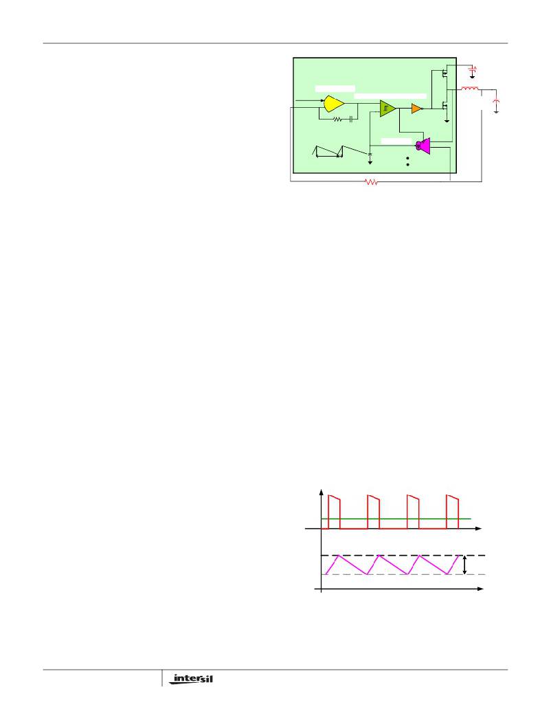
�SYNTHETIC� RIPPLE� REGULATION�
�SIMPLIFIED� DIAGRAM�
�ERROR AMP�
�Vref(DAC)� WINDOW COMPARATOR�
�+�
�-�
�INPUT� VOLTAGE�
�Lo�
�OUTPUT�
�VOLTAGE�
�+�
�Gm� Vout� ,� off�
�{�
�the� expected� XScale� load� and� voltage� transitions� when� used�
�with� the� recommended� 4.7μH� output� inductor� and� 10μF�
�output� capacitor.� Using� the� ISL6271A� evaluation� board,� a�
�50K� feedback� resistor� resulted� in� a� minimum� of� 60� degrees�
�of� phase� margin� under� worst� case� line� and� load� transitions.�
�When� placing� the� Rcomp� feedback� resistor,� be� sure� to� avoid�
�Rc� Cc�
�RIPPLE� CAPACITOR�
�VOLTAGE�
�toff� ton�
�SINK/SOURCE�
�CONTROL�
�Gm AMP�
�-�
�Cr�
�Iout� =� Gm� (� Vin� -� Vout� ),� on�
�routing� it� parallel� to� switching� circuits,� especially� the� phase�
�node,� that� could� otherwise� induce� noise� into� the� FB� pin.�
�Rcomp�
�FIGURE� 20.� SIMPLIFIED� SRR� DIAGRAM�
�(� Rc� ?� Cc� ?� s� +� 1� )�
�Rcomp� ?� Cc� ?� s�
�Gcomp� =� --------------------------------------------�
�(EQ.� 2)�
�Figure� 20� illustrates� the� two� control� loops� inherent� to� the�
�SRR� architecture.� The� inner� loop� consists� of� the� ripple�
�Overcurrent� Protection� and� Ripple� Current�
�The� OCL� trip� level� inside� the� ISL6271A� is� a� function� of� the�
�upper� PMOS� output� transistor� ’s� on-resistance� and� over-�
�current� comparator� threshold� voltage.� The� device� was�
�designed� to� accommodate� a� maximum� RMS� current� of�
�800mA,� and� to� accommodate� this� DC� current� level� plus� the�
�associated� ripple� current,� the� OC� limit� of� the� ISL6271A� will�
�not� trip� below� 950mA.� Ripple� current� inside� the� ISL6271A� is�
�defined� by� the� expression,�
�amplifier,� the� window� comparator,� gate� drive� circuitry� and� the�
�power� stage.� The� outer� loop� controls� the� inner� loop� and� is�
�made� up� a� high� bandwidth� error� amplifier� with� internal� and�
�external� compensation.�
�CCM� Operation� -� Heavy� Current�
�Figure� 21� illustrates� the� SSR� in� CCM.� When� the� upper�
�P-MOSFET� is� turned� on,� the� phase� voltage� equals� the� input�
�voltage� and� the� ripple� transconductance� amplifier� outputs� a�
�current� proportional� to� the� difference� of� the� input� and� output�
�Iripple� =� ----------------------------------� ?� -------------�
�(� Vin� –� Vout� )� Vout�
�L� ?� fs� Vin�
�(EQ.� 3)�
�voltage.� This� current� will� ramp� the� voltage� on� the� ripple�
�capacitor� Cr� in� Figure� 20.� As� this� voltage� reaches� the� upper�
�threshold� of� the� hysteretic� comparator,� the� comparator�
�where� “fs”� is� the� switching� frequency� of� the� converter.� The�
�architecture� of� the� ISL6271A� is� such� that� the� switching�
�frequency� will� increase� with� higher� input� voltage.� This�
�behavior� attempts� to� keep� the� ripple� current� constant� for� a�
�given� output� inductor,� input� voltage� and� output� voltage.� To�
�minimize� ripple� current� and� preserve� transient� response,�
�Intersil� recommends� an� output� inductor� between� 3.3μH� and�
�4.7μH.� Higher� values� of� inductance� will� minimize� the� risk� of�
�tripling� the� over-current� minimum� threshold� of� 950mA.�
�SSR� Theoretical� Operation�
�output� will� switch� low.� After� a� propagation� delay,� the� upper�
�P-MOSFET� is� turned� off� and� the� lower� N-MOSFET� is� turned�
�on,� forcing� synchronous� rectification.� At� this� point,� the� ripple�
�amplifier� now� has� inputs� of� 0V� and� VOUT� and� will� sink�
�current� to� discharge� the� ripple� capacitor.� When� the� voltage�
�across� the� ripple� capacitor� reaches� the� lower� threshold� of�
�the� hysteresis� window,� the� window� comparator� outputs� a�
�high� signal.� After� a� propagation� delay,� the� upper� P-MOSFET�
�turns� on� repeating� the� previous� switching� cycle.�
�The� ISL6271A� is� a� PWM� controller� that� uses� a� novel�
�architecture� developed� by� Intersil� called� Synthetic� Ripple�
�Regulation� .� The� architecture� operates� similar� to� a� hysteretic�
�converter� without� the� deficiencies� of� noise� sensitivities.�
�Reduced� to� its� simplest� form,� the� Synthetic� Ripple� Regulator�
�inside� the� ISL6271A� is� made� up� of� three� elements� as�
�illustrated� in� Figure� 20:� A� transconductance� amplifier�
�(Rippler� Amplifier),� a� window� comparator� with� hysteresis� and�
�an� Error� Amplifier.� While� operating� in� continuous� conduction�
�mode,� the� converter� has� a� natural� switching� frequency� of�
�PHASE�
�VOLTAGE�
�VRP�
�VOUT�
�HYSTERESIS�
�WINDOW�
�1.2MHz� delivering� an� ultra� low� output� voltage� ripple� and�
�exceptional� transient� response� as� illustrated� in� Figures� 23�
�and� 24.�
�12�
�FIGURE� 21.� SYNTHETIC� RIPPLE� REGULATION� IN� CCM�
�FN9171.1�
�相关PDF资料 |
PDF描述 |
|---|---|
| GEM18DRTF | CONN EDGECARD 36POS DIP .156 SLD |
| V150C28E150B2 | CONVERTER MOD DC/DC 28V 150W |
| 1-862545-7 | LEAD ASSY 16AWG SNG END 127MM |
| Q5-3X-1 1/2-01-SS25M | HEATSK DL WL Q53X 1-1/2"X25M BLK |
| VI-B3P-EX | CONVERTER MOD DC/DC 13.8V 75W |
相关代理商/技术参数 |
参数描述 |
|---|---|
| ISL6271ACR-T | 功能描述:IC PMIC XSCALE PROCESSOR 20-QFN RoHS:否 类别:集成电路 (IC) >> PMIC - 电源管理 - 专用 系列:- 应用说明:Ultrasound Imaging Systems Application Note 产品培训模块:Lead (SnPb) Finish for COTS Obsolescence Mitigation Program 标准包装:37 系列:- 应用:医疗用超声波成像,声纳 电流 - 电源:- 电源电压:2.37 V ~ 6 V 工作温度:0°C ~ 70°C 安装类型:表面贴装 封装/外壳:56-WFQFN 裸露焊盘 供应商设备封装:56-TQFN-EP(8x8) 包装:管件 |
| ISL6271ACRZ | 功能描述:直流/直流开关调节器 LD PLL & SRAMG FOR I NTEL PROCESSORS IBM RoHS:否 制造商:International Rectifier 最大输入电压:21 V 开关频率:1.5 MHz 输出电压:0.5 V to 0.86 V 输出电流:4 A 输出端数量: 最大工作温度: 安装风格:SMD/SMT 封装 / 箱体:PQFN 4 x 5 |
| ISL6271ACRZ-T | 功能描述:直流/直流开关调节器 LD PLL & SRAMG FOR I NTEL PROCESSORS IBM RoHS:否 制造商:International Rectifier 最大输入电压:21 V 开关频率:1.5 MHz 输出电压:0.5 V to 0.86 V 输出电流:4 A 输出端数量: 最大工作温度: 安装风格:SMD/SMT 封装 / 箱体:PQFN 4 x 5 |
| ISL6271AEVAL1 | 功能描述:EVALUATION BOARD FOR ISL6271A RoHS:否 类别:编程器,开发系统 >> 评估板 - DC/DC 与 AC/DC(离线)SMPS 系列:- 产品培训模块:Obsolescence Mitigation Program 标准包装:1 系列:True Shutdown™ 主要目的:DC/DC,步升 输出及类型:1,非隔离 功率 - 输出:- 输出电压:- 电流 - 输出:1A 输入电压:2.5 V ~ 5.5 V 稳压器拓扑结构:升压 频率 - 开关:3MHz 板类型:完全填充 已供物品:板 已用 IC / 零件:MAX8969 |
| ISL6271CR | 制造商:Rochester Electronics LLC 功能描述:PLL & SRAM REGULATOR FOR INTEL PROCESSORS - Bulk 制造商:Intersil Corporation 功能描述: |
发布紧急采购,3分钟左右您将得到回复。