参数资料
| 型号: | ISL6561CR-T |
| 厂商: | Intersil |
| 文件页数: | 21/26页 |
| 文件大小: | 0K |
| 描述: | IC CTRLR PWM MULTIPHASE 40-QFN |
| 标准包装: | 4,000 |
| 应用: | 控制器,Intel VR10X |
| 输入电压: | 3 V ~ 12 V |
| 输出数: | 4 |
| 输出电压: | 0.84 V ~ 1.6 V |
| 工作温度: | 0°C ~ 70°C |
| 安装类型: | 表面贴装 |
| 封装/外壳: | 40-VFQFN 裸露焊盘 |
| 供应商设备封装: | 40-QFN(6x6) |
| 包装: | 带卷 (TR) |
�� �
�
�ISL6561�
�In� Equation� 22,� make� sure� that� ?� T� 2� is� the� desired� temperature�
�rise� above� the� ambient� temperature,� and� ?� T� 1� is� the� measured�
�temperature� rise� above� the� ambient� temperature.� While� a�
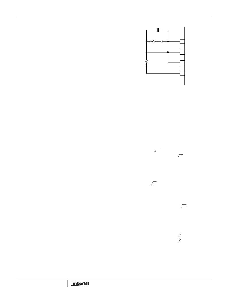
�C� 2� (OPTIONAL)�
�single� adjustment� according� to� Equation� 22� is� usually�
�sufficient,� it� may� occasionally� be� necessary� to� adjust� R� ISEN�
�R� C�
�C� C�
�COMP�
�two� or� more� times� to� achieve� optimal� thermal� balance�
�between� all� channels.�
�FB�
�Load-Line� Regulation� Resistor�
�The� load-line� regulation� resistor� is� labeled� R� FB� in� Figure� 7.�
�Its� value� depends� on� the� desired� full-load� droop� voltage�
�(V� DROOP� in� Figure� 7).� If� Equation� 21� is� used� to� select� each�
�R� FB�
�+�
�V� DROOP�
�-�
�IDROOP�
�VDIFF�
�ISEN� resistor,� the� load-line� regulation� resistor� is� as� shown�
�in� Equation� 23.�
�V� DROOP�
�–� 6�
�R� FB� =� -------------------------�
�70� � 10�
�(EQ.� 23)�
�FIGURE� 13.� COMPENSATION� CONFIGURATION� FOR�
�LOAD-LINE� REGULATED� ISL6561� CIRCUIT�
�If� one� or� more� of� the� ISEN� resistors� is� adjusted� for� thermal�
�balance,� as� in� Equation� 23,� the� load-line� regulation� resistor�
�should� be� selected� according� to� Equation� 24� where� I� FL� is� the�
�full-load� operating� current� and� R� ISEN(n)� is� the� ISEN� resistor�
�connected� to� the� n� th� ISEN� pin.�
�The� feedback� resistor,� R� FB� ,� has� already� been� chosen� as�
�outlined� in� Load-Line� Regulation� Resistor� .� Select� a� target�
�bandwidth� for� the� compensated� system,� f� 0� .� The� target�
�bandwidth� must� be� large� enough� to� assure� adequate�
�transient� performance,� but� smaller� than� 1/3� of� the� per-�
�channel� switching� frequency.� The� values� of� the�
�R� FB� =� --------------------------------�
�V� DROOP�
�I� FL� r� DS� (� ON� )�
�∑� R� ISEN� (� n� )�
�n�
�(EQ.� 24)�
�compensation� components� depend� on� the� relationships� of� f� 0�
�to� the� L-C� pole� frequency� and� the� ESR� zero� frequency.� For�
�each� of� the� three� cases� which� follow,� there� is� a� separate� set�
�of� equations� for� the� compensation� components.�
�-------------------� >� f� 0�
�2� π� f� 0� V� pp� LC�
�0.75V� IN�
�C� C� =� ------------------------------------�
�-------------------� ≤� f� 0� <� ------------------------------�
�Compensation�
�The� two� opposing� goals� of� compensating� the� voltage�
�regulator� are� stability� and� speed.� Depending� on� whether� the�
�regulator� employs� the� optional� load-line� regulation� as�
�described� in� Load-Line� Regulation,� there� are� two� distinct�
�methods� for� achieving� these� goals.�
�COMPENSATING� LOAD-LINE� REGULATED�
�CONVERTER�
�The� load-line� regulated� converter� behaves� in� a� similar�
�Case� 1:�
�Case� 2:�
�1�
�2� π� LC�
�R� C� =� R� FB� ------------------------------------�
�0.75V� IN�
�2� π� V� PP� R� FB� f� 0�
�1� 1�
�2� π� LC� 2� π� C� (� ESR� )�
�V� PP� (� 2� π� )� 2� f� 02� LC�
�R� C� =� R� FB� --------------------------------------------�
�0.75� V�
�0.75V� IN�
�C� C� =� -------------------------------------------------------------�
�PP� R� FB� LC�
�(� 2� π� )� 2� f� 2� V�
�manner� to� a� peak-current� mode� controller� because� the� two�
�poles� at� the� output-filter� L-C� resonant� frequency� split� with�
�the� introduction� of� current� information� into� the� control� loop.�
�The� final� location� of� these� poles� is� determined� by� the� system�
�function,� the� gain� of� the� current� signal,� and� the� value� of� the�
�0�
�IN�
�(EQ.� 25)�
�f� 0� >� ------------------------------�
�2� π� f� 0� V� pp� L�
�0.75� V� IN� (� ESR� )�
�0.75V� IN� (� ESR� )� C�
�2� π� V� PP� R� FB� f� 0� L�
�compensation� components,� R� C� and� C� C� .�
�Since� the� system� poles� and� zero� are� effected� by� the� values�
�of� the� components� that� are� meant� to� compensate� them,� the�
�solution� to� the� system� equation� becomes� fairly� complicated.�
�Fortunately� there� is� a� simple� approximation� that� comes� very�
�close� to� an� optimal� solution.� Treating� the� system� as� though� it�
�were� a� voltage-mode� regulator� by� compensating� the� L-C�
�poles� and� the� ESR� zero� of� the� voltage-mode� approximation�
�Case� 3:�
�1�
�2� π� C� (� ESR� )�
�R� C� =� R� FB� ------------------------------------------�
�C� C� =� -------------------------------------------------�
�yields� a� solution� that� is� always� stable� with� very� close� to� ideal�
�transient� performance.�
�21�
�In� Equations� 25,� L� is� the� per-channel� filter� inductance�
�divided� by� the� number� of� active� channels;� C� is� the� sum� total�
�of� all� output� capacitors;� ESR� is� the� equivalent-series�
�resistance� of� the� bulk� output-filter� capacitance;� and� V� PP� is�
�the� peak-to-peak� sawtooth� signal� amplitude� as� described� in�
�Figure� 6� and� Electrical� Specifications� .�
�FN9098.5�
�May� 12,� 2005�
�相关PDF资料 |
PDF描述 |
|---|---|
| ISL6563IR-T | IC CTRLR PWM MULTIPHASE 24-QFN |
| ISL6564AIRZ | IC REG CTRLR BUCK PWM VM 40-QFN |
| ISL6564IR-T | IC REG CTRLR BUCK PWM VM 40-QFN |
| ISL6565BCV-T | IC REG CTRLR BUCK PWM VM 28TSSOP |
| ISL6566AIRZ | IC CTRLR PWM 3PHASE BUCK 40-QFN |
相关代理商/技术参数 |
参数描述 |
|---|---|
| ISL6561CRZ | 功能描述:IC CTRLR PWM MULTIPHASE 40-QFN RoHS:是 类别:集成电路 (IC) >> PMIC - 稳压器 - 专用型 系列:- 标准包装:43 系列:- 应用:控制器,Intel VR11 输入电压:5 V ~ 12 V 输出数:1 输出电压:0.5 V ~ 1.6 V 工作温度:-40°C ~ 85°C 安装类型:表面贴装 封装/外壳:48-VFQFN 裸露焊盘 供应商设备封装:48-QFN(7x7) 包装:管件 |
| ISL6561CRZ | 制造商:Intersil Corporation 功能描述:Pulse Width Modulation (PWM) Controller |
| ISL6561CRZA | 功能描述:IC CTRLR PWM MULTIPHASE 40-QFN RoHS:是 类别:集成电路 (IC) >> PMIC - 稳压器 - 专用型 系列:- 标准包装:43 系列:- 应用:控制器,Intel VR11 输入电压:5 V ~ 12 V 输出数:1 输出电压:0.5 V ~ 1.6 V 工作温度:-40°C ~ 85°C 安装类型:表面贴装 封装/外壳:48-VFQFN 裸露焊盘 供应商设备封装:48-QFN(7x7) 包装:管件 |
| ISL6561CRZA-T | 功能描述:IC CTRLR PWM MULTIPHASE 40-QFN RoHS:是 类别:集成电路 (IC) >> PMIC - 稳压器 - 专用型 系列:- 标准包装:43 系列:- 应用:控制器,Intel VR11 输入电压:5 V ~ 12 V 输出数:1 输出电压:0.5 V ~ 1.6 V 工作温度:-40°C ~ 85°C 安装类型:表面贴装 封装/外壳:48-VFQFN 裸露焊盘 供应商设备封装:48-QFN(7x7) 包装:管件 |
| ISL6561CRZR5208 | 制造商:Rochester Electronics LLC 功能描述: 制造商:Intersil Corporation 功能描述: |
发布紧急采购,3分钟左右您将得到回复。