- 您现在的位置:买卖IC网 > PDF目录15181 > ISL6567IRZ-TS2698 (Intersil)IC REG CTRLR BUCK PWM VM 24-QFN PDF资料下载
参数资料
| 型号: | ISL6567IRZ-TS2698 |
| 厂商: | Intersil |
| 文件页数: | 20/25页 |
| 文件大小: | 0K |
| 描述: | IC REG CTRLR BUCK PWM VM 24-QFN |
| 标准包装: | 6,000 |
| PWM 型: | 电压模式 |
| 输出数: | 1 |
| 频率 - 最大: | 1.5MHz |
| 占空比: | 66% |
| 电源电压: | 4.9 V ~ 5.5 V |
| 降压: | 是 |
| 升压: | 无 |
| 回扫: | 无 |
| 反相: | 无 |
| 倍增器: | 无 |
| 除法器: | 无 |
| Cuk: | 无 |
| 隔离: | 无 |
| 工作温度: | -40°C ~ 85°C |
| 封装/外壳: | 24-VFQFN 裸露焊盘 |
| 包装: | 带卷 (TR) |
�� �
�
�ISL6567�
�Δ� V� ≈� (� ESL� )� -----� +� (� ESR� )� Δ� I�
�peak� dependent� on� the� quality� factor� (Q)� of� the� output� filter,�
�which� is� not� shown.� Using� the� above� guidelines� should� yield� a�
�compensation� gain� similar� to� the� curve� plotted.� The� open� loop�
�error� amplifier� gain� bounds� the� compensation� gain.� Check� the�
�compensation� gain� at� F� P2� against� the� capabilities� of� the� error�
�amplifier.� The� closed� loop� gain,� G� CL� ,� is� constructed� on� the�
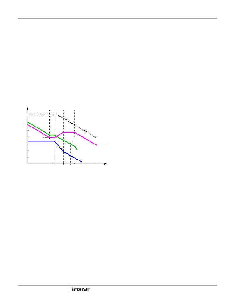
�log-log� graph� of� Figure� 25� by� adding� the� modulator� gain,� G� MOD�
�(in� dB),� to� the� feedback� compensation� gain,� G� FB� (in� dB).� This� is�
�equivalent� to� multiplying� the� modulator� transfer� function� and�
�the� compensation� transfer� function� and� then� plotting� the�
�resulting� gain.� A� stable� control� loop� has� a� gain� crossing� with� close�
�to� a� -20dB/decade� slope� and� a� phase� margin� greater� than� 45°.�
�Include� worst� case� component� variations� when� determining�
�phase� margin.� The� mathematical� model� presented� makes� a�
�number� of� approximations� and� is� generally� not� accurate� at�
�frequencies� approaching� or� exceeding� half� the� switching�
�frequency.� When� designing� compensation� networks,� select� target�
�crossover� frequencies� in� the� range� of� 10%� to� 30%� of� the� per-�
�channel� switching� frequency,� F� SW� .�
�At� the� beginning� of� the� load� transient,� the� output� capacitors�
�supply� all� of� the� transient� current.� The� output� voltage� will�
�initially� deviate� by� an� amount� approximated� by� the� voltage�
�drop� across� the� ESL.� As� the� load� current� increases,� the� voltage�
�drop� across� the� ESR� increases� linearly� until� the� load� current�
�reaches� its� final� value.� The� capacitors� selected� must� have�
�sufficiently� low� ESL� and� ESR� so� that� the� total� output� voltage�
�deviation� is� less� than� the� allowable� maximum.� Neglecting� the�
�contribution� of� inductor� current� and� regulator� response,� the�
�output� voltage� initially� deviates� according� to� Equation� 21.�
�di� (EQ.� 21)�
�dt�
�The� filter� capacitor� must� have� sufficiently� low� ESL� and� ESR� so�
�that� Δ� V� <� Δ� V� MAX� .�
�Most� capacitor� solutions� rely� on� a� mixture� of� high-frequency�
�capacitors� with� relatively� low� capacitance� in� combination� with�
�bulk� capacitors� having� high� capacitance� but� limited� high-�
�frequency� performance.� Minimizing� the� ESL� of� the� high-�
�F� Z1� F� Z2�
�F� P1�
�F� P2�
�MODULATOR� GAIN�
�COMPENSATION� GAIN�
�frequency� capacitors� allows� them� to� support� the� output�
�voltage� as� the� current� increases.� Minimizing� the� ESR� of� the�
�CLOSED� LOOP� GAIN�
�OPEN� LOOP� E/A� GAIN�
�bulk� capacitors� allows� them� to� supply� the� increased� current�
�with� less� output� voltage� deviation.�
�The� ESR� of� the� bulk� capacitors� is� also� responsible� for� the�
�majority� of� the� output-voltage� ripple.� As� the� bulk� capacitors�
�20� log� ?� --------� ?�
�OSC�
�0�
�R2�
�?� R1� ?�
�d� MAX� ?� V� IN�
�20� log� --------------------------------�
�V�
�G� CL�
�G� FB�
�sink� and� source� the� inductor� AC� ripple� current,� a� voltage�
�develops� across� the� bulk-capacitor� ESR� equal� to� I� PP� .� Thus,�
�once� the� output� capacitors� are� selected� and� a� maximum�
�allowable� ripple� voltage,� V� PP(MAX)� ,� is� determined� from� an�
�analysis� of� the� available� output� voltage� budget,� Equation� 22�
�can� be� used� to� determine� a� lower� limit� on� the� output�
�(� V� IN� –� 2� ?� V� OUT� )� ?� V� OUT�
�f� S� ?� V� IN� ?� V� PP� (� MAX� )�
�LOG�
�F� LC�
�F� CE�
�F� 0�
�G� MOD�
�FREQUENCY�
�inductance.�
�L� ≥� ESR� ?� ----------------------------------------------------------�
�(EQ.� 22)�
�L� ≤� -----------------------------� ?� (� Δ� V� MAX� –� Δ� I� ?� ESR� )�
�4� ?� C� ?� V� OUT�
�(EQ.� 23)�
�(� Δ� I� )�
�L� ≤� ----------------� ?� (� Δ� V� MAX� –� Δ� I� ?� ESR� )� ?� (� V� IN� –� V� O� )�
�2.5� ?� C�
�(EQ.� 24)�
�(� Δ� I� )�
�FIGURE� 25.� ASYMPTOTIC� BODE� PLOT� OF� CONVERTER� GAIN�
�OUTPUT� FILTER� DESIGN�
�The� output� inductors� and� the� output� capacitor� bank� together�
�form� a� low-pass� filter� responsible� for� smoothing� the� square�
�wave� voltage� at� the� phase� nodes.� Additionally,� the� output�
�capacitors� must� also� provide� the� energy� required� by� a� fast�
�transient� load� during� the� short� interval� of� time� required� by� the�
�controller� and� power� train� to� respond.� Because� it� has� a� low�
�bandwidth� compared� to� the� switching� frequency,� the� output�
�filter� limits� the� system� transient� response� leaving� the� output�
�capacitor� bank� to� supply� the� load� current� or� sink� the� inductor�
�currents,� all� while� the� current� in� the� output� inductors� increases�
�or� decreases� to� meet� the� load� demand.�
�In� high-speed� converters,� the� output� capacitor� bank� is�
�amongst� the� costlier� (and� often� the� physically� largest)� parts� of�
�the� circuit.� Output� filter� design� begins� with� consideration� of� the�
�critical� load� parameters:� maximum� size� of� the� load� step,� Δ� I,�
�the� load-current� slew� rate,� di/dt,� and� the� maximum� allowable�
�output� voltage� deviation� under� transient� loading,� Δ� V� MAX� .�
�Capacitors� are� characterized� according� to� their� capacitance,�
�ESR,� and� ESL� (equivalent� series� inductance).�
�20�
�Since� the� capacitors� are� supplying� a� decreasing� portion� of� the�
�load� current� while� the� regulator� recovers� from� the� transient,�
�the� capacitor� voltage� becomes� slightly� depleted.� The� output�
�inductors� must� be� capable� of� assuming� the� entire� load� current�
�before� the� output� voltage� decreases� more� than� Δ� V� MAX� .� This�
�places� an� upper� limit� on� inductance.�
�2�
�While� Equation� 23� addresses� the� leading� edge,� Equation� 24�
�gives� the� upper� limit� on� L� for� cases� where� the� trailing� edge� of�
�the� current� transient� causes� a� greater� output� voltage� deviation�
�than� the� leading� edge.�
�2�
�Normally,� the� trailing� edge� dictates� the� selection� of� L,� if� the�
�duty� cycle� is� less� than� 50%.� Nevertheless,� both� inequalities�
�should� be� evaluated,� and� L� should� be� selected� based� on� the�
�lower� of� the� two� results.� In� all� equations� in� this� paragraph,� L� is�
�the� per-channel� inductance� and� C� is� the� total� output� bulk�
�capacitance.�
�FN9243.4�
�August� 9,� 2011�
�相关PDF资料 |
PDF描述 |
|---|---|
| ISL6567IRZ-T | IC REG CTRLR BUCK PWM VM 24-QFN |
| B41041A6158M | 1500UF 50V 16X35.5 SINGLE END |
| ISL6522IVZ | IC REG CTRLR BST PWM VM 14-TSSOP |
| ASC15DRTN | CONN EDGECARD 30POS .100 DIP SLD |
| H2ABT-10110-S4-ND | JUMPER-H1502TR/A2015S/H1500TR10" |
相关代理商/技术参数 |
参数描述 |
|---|---|
| ISL6568CR | 功能描述:IC CTRLR PWM BUCK 2PHASE 32-QFN RoHS:否 类别:集成电路 (IC) >> PMIC - 稳压器 - 专用型 系列:- 产品培训模块:Lead (SnPb) Finish for COTS Obsolescence Mitigation Program 标准包装:2,000 系列:- 应用:电源,ICERA E400,E450 输入电压:4.1 V ~ 5.5 V 输出数:10 输出电压:可编程 工作温度:-40°C ~ 85°C 安装类型:表面贴装 封装/外壳:42-WFBGA,WLCSP 供应商设备封装:42-WLP 包装:带卷 (TR) |
| ISL6568CR-T | 功能描述:IC CTRLR PWM BUCK 2PHASE 32-QFN RoHS:否 类别:集成电路 (IC) >> PMIC - 稳压器 - 专用型 系列:- 产品培训模块:Lead (SnPb) Finish for COTS Obsolescence Mitigation Program 标准包装:2,000 系列:- 应用:电源,ICERA E400,E450 输入电压:4.1 V ~ 5.5 V 输出数:10 输出电压:可编程 工作温度:-40°C ~ 85°C 安装类型:表面贴装 封装/外壳:42-WFBGA,WLCSP 供应商设备封装:42-WLP 包装:带卷 (TR) |
| ISL6568CRZ | 制造商:Intersil Corporation 功能描述:CURRENT MODE PWM CNTRLR 0.8375V TO 12V 60A 32QFN EP - Rail/Tube 制造商:Intersil 功能描述:2-PH PWM CNTRLR VRM9 W/2-DRVRS 10 K8 DAC |
| ISL6568CRZA | 制造商:Intersil Corporation 功能描述:CURRENT MODE PWM CNTRLR 0.8375V TO 12V 60A 32QFN EP - Rail/Tube 制造商:Intersil 功能描述:W/ANNEAL 2-PH PWM CNTRLR 2-DRVRS VRM9 |
| ISL6568CRZA-T | 制造商:Intersil Corporation 功能描述:CURRENT MODE PWM CNTRLR 0.8375V TO 12V 60A 32QFN EP - Tape and Reel 制造商:Intersil 功能描述:W/ANNEAL 2-PHS PWM CNTRLR W/2-DRVRS |
发布紧急采购,3分钟左右您将得到回复。